
electronics-journal.com
10
'26
Written on Modified on
High-Volume Processing of 300-Millimeter Silicon Carbide Substrates
Infineon has successfully fabricated functional power devices on larger wafer formats, expanding wide-bandgap production capacity for automotive and industrial energy conversion systems.
www.infineon.com
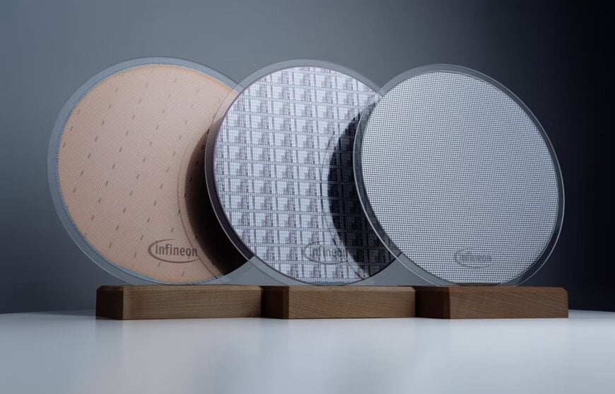
Infineon now masters all three materials in 300 mm: silicon, silicon carbide and gallium nitride.
Infineon Technologies has produced functional power devices on 300-millimeter silicon carbide (SiC) wafers, introducing a dimensional scale-up in semiconductor manufacturing. This hardware milestone is engineered to supply high-voltage components for electric vehicle traction inverters, renewable energy storage, and solid-state transformers within artificial intelligence data centers.
Wafer Dimensional Scaling and Fabrication Integration
The transition from the current 200-millimeter baseline to a 300-millimeter format yields approximately 2.3 times more semiconductor chips per wafer. The initial functional devices were processed at the company's facility in Villach, Austria. This production run was executed by adapting existing 300-millimeter silicon (Si) manufacturing equipment to accommodate the distinct thermodynamic and chemical properties of silicon carbide. Utilizing established high-volume silicon toolsets allows for an accelerated industrialization timeline and stabilizes the global supply chain for high-power components.
Material Cleaving and Yield Optimization
In parallel with device fabrication, the company validated its Cold Split technology for 300-millimeter SiC boules at its Dresden, Germany site. Traditional SiC wafering relies on mechanical wire sawing, which generates substantial kerf loss—wasting valuable crystalline material as dust. The Cold Split method uses laser-induced stress to cleave the wafers from the boule, significantly reducing material waste and shortening processing time. This structural separation technique maximizes the yield of usable substrates from a single crystal, lowering the capital expenditure required per processed wafer.
Wide-Bandgap Application Ecosystem
Silicon carbide is a critical material for high-efficiency power conversion. Compared to standard silicon, SiC’s wider bandgap enables lower switching losses, higher power density, and stable operation under elevated thermal and voltage loads. These electrical characteristics are strictly required for high-capacity on-board chargers, industrial drives, and continuous power supply units. The processed 300-millimeter SiC wafers are exhibited at the electronica trade show, scheduled for November 10–13, 2026, in Munich, Germany.
Additional Context
This section details technical specifications and competitive benchmarking not included in the original news release.
Within the wide-bandgap semiconductor market, the prevailing manufacturing standard for silicon carbide utilizes 200-millimeter (8-inch) substrates. Competitors such as Wolfspeed, STMicroelectronics, and Onsemi have recently consolidated their primary fabrication architectures around the 200-millimeter standard to improve die yield and economies of scale. Scaling to a 300-millimeter (12-inch) SiC architecture presents a severe material engineering challenge, primarily due to the thermodynamic difficulty of growing defect-free SiC boules at larger diameters without introducing basal plane dislocations.
By successfully processing at the 300-millimeter scale, the available geometric surface area increases by 130% compared to 200-millimeter benchmarks. This dimensional expansion directly targets the high cost-per-die ratio that historically limits SiC integration in cost-sensitive electric vehicle and industrial automation architectures.
Edited by Aishwarya Mambet, Induportals Editor, with AI assistance.
www.infineon.com
Infineon Technologies has produced functional power devices on 300-millimeter silicon carbide (SiC) wafers, introducing a dimensional scale-up in semiconductor manufacturing. This hardware milestone is engineered to supply high-voltage components for electric vehicle traction inverters, renewable energy storage, and solid-state transformers within artificial intelligence data centers.
Wafer Dimensional Scaling and Fabrication Integration
The transition from the current 200-millimeter baseline to a 300-millimeter format yields approximately 2.3 times more semiconductor chips per wafer. The initial functional devices were processed at the company's facility in Villach, Austria. This production run was executed by adapting existing 300-millimeter silicon (Si) manufacturing equipment to accommodate the distinct thermodynamic and chemical properties of silicon carbide. Utilizing established high-volume silicon toolsets allows for an accelerated industrialization timeline and stabilizes the global supply chain for high-power components.
Material Cleaving and Yield Optimization
In parallel with device fabrication, the company validated its Cold Split technology for 300-millimeter SiC boules at its Dresden, Germany site. Traditional SiC wafering relies on mechanical wire sawing, which generates substantial kerf loss—wasting valuable crystalline material as dust. The Cold Split method uses laser-induced stress to cleave the wafers from the boule, significantly reducing material waste and shortening processing time. This structural separation technique maximizes the yield of usable substrates from a single crystal, lowering the capital expenditure required per processed wafer.
Wide-Bandgap Application Ecosystem
Silicon carbide is a critical material for high-efficiency power conversion. Compared to standard silicon, SiC’s wider bandgap enables lower switching losses, higher power density, and stable operation under elevated thermal and voltage loads. These electrical characteristics are strictly required for high-capacity on-board chargers, industrial drives, and continuous power supply units. The processed 300-millimeter SiC wafers are exhibited at the electronica trade show, scheduled for November 10–13, 2026, in Munich, Germany.
Additional Context
This section details technical specifications and competitive benchmarking not included in the original news release.
Within the wide-bandgap semiconductor market, the prevailing manufacturing standard for silicon carbide utilizes 200-millimeter (8-inch) substrates. Competitors such as Wolfspeed, STMicroelectronics, and Onsemi have recently consolidated their primary fabrication architectures around the 200-millimeter standard to improve die yield and economies of scale. Scaling to a 300-millimeter (12-inch) SiC architecture presents a severe material engineering challenge, primarily due to the thermodynamic difficulty of growing defect-free SiC boules at larger diameters without introducing basal plane dislocations.
By successfully processing at the 300-millimeter scale, the available geometric surface area increases by 130% compared to 200-millimeter benchmarks. This dimensional expansion directly targets the high cost-per-die ratio that historically limits SiC integration in cost-sensitive electric vehicle and industrial automation architectures.
Edited by Aishwarya Mambet, Induportals Editor, with AI assistance.
www.infineon.com
