
electronics-journal.com
14
'26
Written on Modified on
Semiconductor Test Pattern Execution High Speed Interfaces
Siemens EDA launches Tessent Silicon Executable software to translate and run design-for-test patterns natively across automated test equipment, bench, and system-level environments.
www.siemens.com
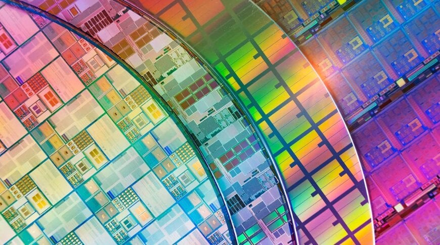
Rising silicon complexity, multi-die architectures, and advanced packaging create severe bottlenecks in test time and scan data delivery across modern semiconductor manufacturing. Siemens EDA addresses this structural challenge through Tessent Silicon Executable, a standalone application engineered to bridge the gap between design-for-test collateral creation and physical silicon bring-up across diverse test hardware platforms.
Bridging Design-for-Test Generation and Physical Silicon Bring-Up
Modern microelectronics — ranging from high-performance computing chiplets to automotive processors — rely heavily on advanced transistor technologies and 2.5D or 3D multi-die packaging. These structural shifts dramatically expand total test content. Traditional pin-limited scan test delivery often fails to deliver adequate bandwidth, leading to excessive test application times and delayed production ramp schedules.
Tessent Silicon Executable operates as an execution bridge. The application ingests collateral generated during pre-silicon design-for-test insertion and pattern generation workflows. Rather than requiring manual translation or proprietary test program re-engineering for different target systems, the software translates scan vectors and applies them directly through the native execution environment of the target hardware. Upon test completion, it feeds physical results straight back into established Tessent debug, failure analysis, and diagnosis pipelines. This bidirectional flow maintains data correlation between design verification, characterization benches, and mass production floors.
Standardizing Pattern Delivery Across Automated Test Equipment Ecosystems
A central technical obstacle in semiconductor test engineering involves the fragmentation between laboratory benches, automated test equipment, system-level test, and in-system operational environments. Engineers often struggle to correlate failure data when test programs undergo multiple rounds of custom reformatting across disparate test instruments.
To eliminate conversion overhead, Siemens EDA established direct integration partnerships with automated test equipment vendors Advantest and Teradyne.
Advantest embeds the software into its V93000 test platform utilizing Link Scale technology, while extending compatibility to pre-silicon verification and laboratory engineering via SiConic. This establishes an unbroken execution path from initial simulation to high-volume wafer probe and package testing.
Teradyne incorporates the application into its UltraPort instrument on the UltraFLEXplus platform. This implementation provides an integrated mechanism to route Siemens Streaming Scan Network data over standard peripheral component interconnect express links, supporting speeds up to PCIe Gen 6. Delivering dense scan test content over high-speed standard serial protocols directly bypasses general-purpose input/output pin constraints and cuts execution duration during advanced package testing.
By unifying execution semantics across automated test equipment, laboratory bring-up benches, and system-level fixtures, the software standardizes defect localization and optimizes overall device manufacturing economics.
Additional Context
This section details technical specifications and competitive benchmarking not included in the original product announcement.
Historically, scan testing depended on dedicated low-speed digital channels provided by automated test equipment pins, structured around IEEE 1149.1 (JTAG) or standard parallel scan chains. As pin count limitations collided with gigabyte-scale pattern volumes in multi-billion-transistor systems-on-chip, the industry turned to packetized scan distribution architectures. Siemens established this trend with its Streaming Scan Network (SSN) technology, designed to decouple core-level test data from chip-level pin constraints through a bus-based transport mechanism.
Competitive and industry alternatives approach high-bandwidth test delivery through varying frameworks. Synopsys addresses high-speed pattern streaming primarily via DesignWare IP interfaces and its proprietary DFTMAX and TestMAX toolchains, routing test data through functional interfaces like USB, PCIe, or Ethernet. Similarly, Cadence Design Systems utilizes Modus DFT Software with elastic compression to stream scan data across functional serial buses.
The industry benchmark differentiator for Tessent Silicon Executable lies in execution layer detachment. Rather than compiling scan patterns into vendor-specific tester vectors prior to loading onto automated test equipment, Tessent Silicon Executable runs directly on the tester workstation or instrument processor. By executing standard protocols such as SSN over PCIe Gen 6, test teams can leverage high-speed functional transceivers capable of 64 GT/s raw transfer rates. This protocol-native delivery eliminates external protocol converters and bridges the operational division between design-stage automated test pattern generation and automated test equipment execution.
Edited by Evgeny Churilov, Induportals Media - Adapted by AI.
www.siemens.com
