
electronics-journal.com
14
'26
Written on Modified on
Broadband Semiconductor Characterization in the Sub-Terahertz Range
Single-touchdown measurements from near DC to 250 GHz accelerate the development of high-frequency transistors for future telecommunications systems.
www.keysight.com
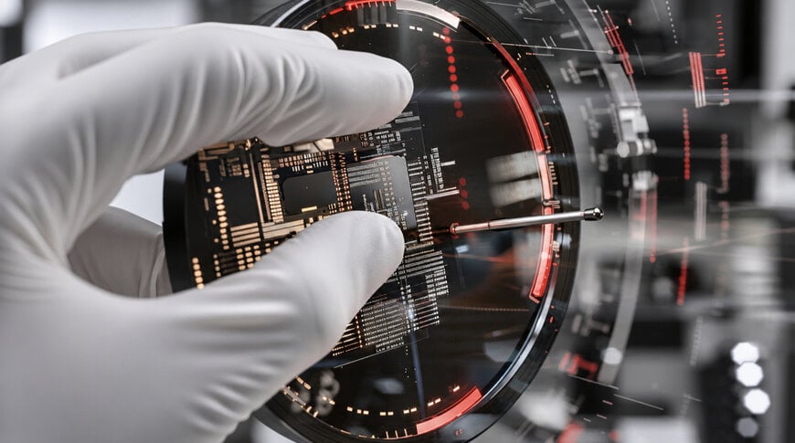
As semiconductor technology advances into the millimeter-wave and sub-terahertz frequency ranges, engineers and development teams face significant measurement challenges. Accurately modeling active devices such as indium phosphide high-electron-mobility transistors (InP HEMTs) requires seamless characterization of their physical properties across extremely wide frequency bands. Traditional test methods often require multiple test setups and time-consuming recalibration across different frequency ranges, increasing complexity and potentially introducing inconsistencies in S-parameter data.
To address these challenges, Keysight Technologies, the University of Glasgow, the National Physical Laboratory, and MPI Corporation have developed a new measurement approach for continuous on-wafer characterization. The integrated approach enables device data to be acquired from near DC to 250 GHz in a single sweep, using a single probe touchdown.
Integrated System Architecture for Measurements up to 250 GHz
The measurement setup integrates instrumentation, on-wafer probing, and metrology expertise into a unified system. At its core is Keysight’s PNA-X vector network analyzer, combined with a specialized 250 GHz single-sweep frequency extender and a precision source measure unit (SMU) for accurate DC biasing.
The measurement hardware is complemented by InP HEMT devices and precision on-wafer calibration standards from the University of Glasgow, along with broadband on-wafer probe technology and calibration software from MPI Corporation. The National Physical Laboratory contributed expertise in high-frequency measurement techniques and metrological calibration. Integrated source filtering and broadband calibration of source power at the probe tip help maintain the spectral purity of the applied millimeter-wave signal.
Technical Performance and Industrial Applications
Continuous data acquisition using a single probe touchdown eliminates potential mechanical and electrical sources of error associated with repeated probe repositioning or changes between measurement setups. This approach improves measurement consistency and supports reproducible S-parameter results across the entire frequency range, from near DC to 250 GHz.
Typical applications include research and industrial development of advanced semiconductors for next-generation communications infrastructure, artificial intelligence systems, radar, and high-frequency electronics. By reducing the need for repeated setup changes, the approach can shorten development cycles for new transistor structures.
Additional Context
This section provides technical specifications and competitive comparisons that were not included in the original product announcement.
The demand for continuous characterization methods in the sub-terahertz range stems from increasing data-rate and bandwidth requirements in advanced communications, including future 6G networks. Conventional measurement systems that divide the frequency range into separate bands can encounter discontinuities at band transitions and additional insertion losses between different frequency modules.
Using directly connected frequency extenders with precision RF connections can reduce signal-path lengths and help preserve system dynamic range. Whereas conventional measurement approaches may rely on complex, segmented calibration procedures, the demonstrated single-sweep approach offers a more efficient method for broadband semiconductor characterization.
Edited by Sucithra Mani, Induportals Editor – adapted with AI assistance.
www.keysight.com
