
electronics-journal.com
24
'26
Written on Modified on
Adaptive High-Bandwidth Memory for Mobile AI
Samsung validates its next-generation LPDDR memory on Qualcomm’s mobile platform to address rising bandwidth and power demands of edge AI.
semiconductor.samsung.com
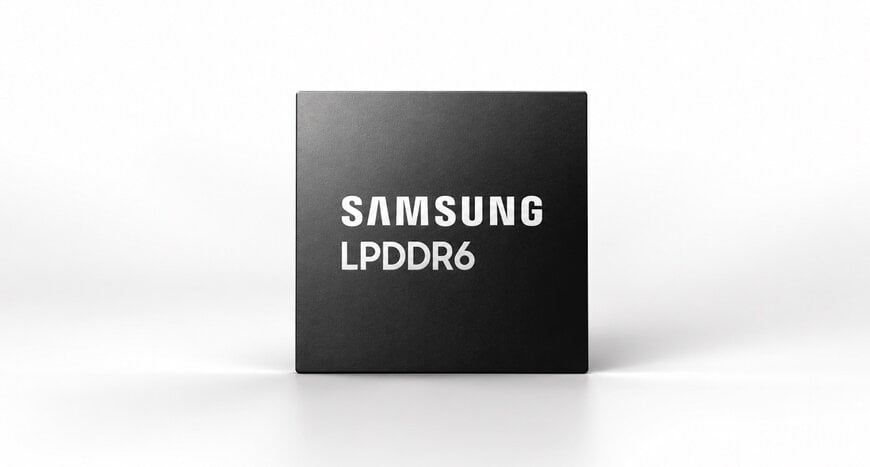
Samsung Electronics has announced the validation of its 16GB LPDDR6 memory module on the Qualcomm Technologies' Snapdragon 8 Elite Extreme Gen 6 mobile platform. The hardware integration addresses the escalating bandwidth and power efficiency requirements of complex, on-device artificial intelligence workloads, specifically large language model (LLM) inference and persistent multimodal AI agents.
Data Movement and Bandwidth Requirements for Edge AI
Mobile computing architectures are transitioning from running standalone, single-function AI features toward managing persistent, context-aware AI agents. During LLM inference on a mobile device, the system processor must continuously access massive model weights and key-value (KV) cache data stored in the system memory. As these generative models scale and user interactions lengthen, the physical movement of data between the memory and the processor creates a significant computational bottleneck.
Samsung developed the LPDDR6 architecture to directly mitigate these data-movement constraints. The memory module utilizes an expanded input/output (I/O) architecture and elevated per-pin transmission speeds to deliver up to 114 GB/s of total memory bandwidth. Operating at I/O speeds up to 10.7 Gbps, this increased throughput allows the mobile system-on-chip (SoC) to fetch required AI processing data more rapidly, reducing latency for responsive, on-device generative tasks.
Adaptive Power Scaling and Data Reliability
While high bandwidth is necessary for AI processing bursts, mobile workloads frequently shift between intensive inference tasks and lighter background operations. Managing these fluctuations within a strict mobile thermal envelope requires dynamic power regulation.
The Samsung LPDDR6 integrates Dynamic Voltage and Frequency Scaling (DVFS) alongside a new Dynamic Efficiency Mode (DEM). DVFS actively modulates the operating voltage and clock frequency based on immediate performance demands, while DEM aggressively reduces power consumption during idle or low-utilization states. This combined adaptive approach improves overall power efficiency by up to 21 percent compared to the previous LPDDR5X generation, preventing the memory from drawing peak power unnecessarily and extending mobile battery life.
Furthermore, intense and prolonged AI processing increases the frequency of memory row activations, which can lead to data interference or degradation. To ensure reliability, LPDDR6 incorporates Per-Row Activation Counting (PRAC). This mechanism actively monitors the repeated activation of specific memory rows to manage and mitigate potential interference patterns, ensuring data integrity during sustained multimodal processing.
Platform Validation
Memory technology requires system-level optimization with the SoC to ensure stability. The successful validation of the 16GB LPDDR6 on the Snapdragon 8 Elite Extreme Gen 6 marks the industry's first LPDDR6 validation on a next-generation mobile platform, confirming the memory's readiness for commercial deployment in advanced AI-capable smartphones and edge devices.
Additional Context
This section details technical specifications and competitive benchmarking not included in the original news release.
The transition to the LPDDR6 standard (formalized by JEDEC) is fiercely contested by the three primary global memory manufacturers: Samsung, SK Hynix, and Micron, alongside emerging competitors such as China's ChangXin Memory Technologies (CXMT).
While Samsung has achieved the first SoC-level validation on Qualcomm's Snapdragon platform, SK Hynix has recently completed the development of its own 1c-process (10nm-class) LPDDR6 memory. SK Hynix’s initial LPDDR6 modules match Samsung’s validated 10.7 Gbps base speed, with mass production slated for the second half of 2026. Simultaneously, CXMT is nearing R&D validation for an LPDDR6 iteration targeting a 12.8 Gbps design specification.
Because the LPDDR6 physical standard is engineered to eventually scale up to 14.4 Gbps, early hardware validation milestones like Samsung's are critical. Transitioning from the 16-bit channel width of LPDDR5X to the dual 12-bit sub-channel (24-bit total) interface of LPDDR6—while lowering the base operating voltage to 0.9V/1.0V—demands tight co-engineering between the memory supplier and the mobile processor designer. By validating its 10.7 Gbps silicon directly on the Snapdragon architecture first, Samsung secures a distinct time-to-market advantage over competitors that are still completing internal die validation and mass-production preparations.
Edited by Aishwarya Mambet, Induportals Editor, with AI assistance.
www.samsung.com
