
electronics-journal.com
06
'26
Written on Modified on
Next-Generation Vertically Stacked Memory Architectures For Artificial Intelligence Infrastructure
Samsung Electronics introduces advanced hybrid bonding technologies and ultra-high-layer storage components to maximize bandwidth efficiency in parallel computing systems.
semiconductor.samsung.com
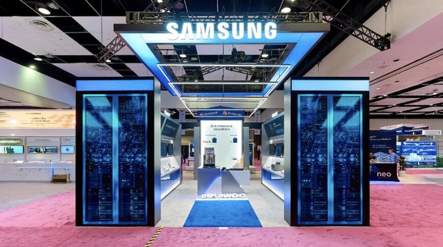
Samsung showcased its latest AI memory innovations at FMS 2026
Samsung Electronics outlined a product timeline for next-generation data storage and retrieval systems, featuring vertically stacked high-bandwidth memory and 400-layer NAND flash logic. These semiconductor solutions aim to resolve data bottleneck issues within high-performance computing centers and enterprise server infrastructure.
System Architecture and Exhibition Overview
At the Future of Memory and Storage 2026 exhibition, held in Santa Clara, California, on August 4, 2026, Samsung presented its 3D memory architecture models. The display included the zHBM and zNAND-O concepts, the V10 BV-NAND storage solution, and an extended product portfolio covering HBM4E, HBM5, LPDDR5X-PIM, and enterprise solid-state drives. During a technical keynote presentation, corporate engineering executives Jin-Yub Lee and Kyungryun Kim detailed how vertical integration and 3D structural innovations function as primary methods to maximize system performance and thermal efficiency across the server memory hierarchy.
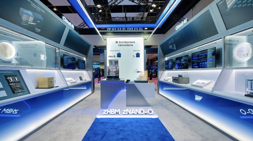
Vertical Memory Integration Over Logic Components
The zHBM memory concept alters traditional 2.5D packaging by stacking high-bandwidth memory vertically and directly on top of artificial intelligence accelerators. Minimizing the physical distance of the data bus between the processor and memory reduces parasitic resistance, providing a mechanism for ultra-fast data transfer with lower power consumption. According to engineering projections, an interface using zHBM yields approximately eight times the bandwidth of standard HBM5 modules. Through the use of advanced wafer bonding techniques, zHBM is designed to reach a memory density 10 times greater than HBM5, while tripling energy efficiency and reducing thermal resistance by more than 50 percent. The architecture accommodates custom intellectual property integration in the base interlayer, allowing system architects to tailor accelerator functionality and memory capacity for specific training workloads.
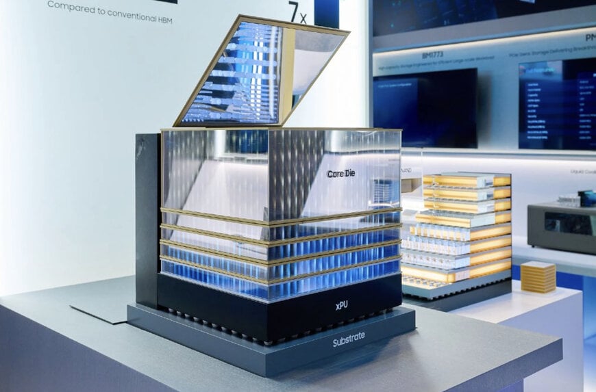
Concept model of Samsung’s HBM
High-Density NAND and Edge Storage Solutions
Addressing local, data-intensive processing, Samsung introduced zNAND-O, an optimized NAND architecture available in four-layer and eight-layer physical configurations. The design focuses on improved input/output throughput and low latency tailored for edge computing environments. For enterprise data tiers, the company unveiled V10 BV-NAND, an architecture incorporating over 400 layers through a proprietary wafer bonding process. This method bonds independently manufactured peripheral circuits and memory cell arrays, achieving a 58 percent increase in storage density compared to the previous V9 generation. In addition to volumetric density, V10 BV-NAND increases read, write, and input/output speeds to support large-scale storage arrays in high-performance computing centers.
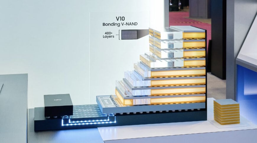
Concept model of Samsung zNAND-O
Processing-in-Memory and Future Component Integration
Samsung showcased samples of HBM4E, which follow the mass production of HBM4 using 1c DRAM and a 4-nanometer base die initiated earlier in the year. To further reduce energy consumed by data movement, the exhibition included LPDDR5X-PIM, a memory module incorporating processing-in-memory technology that executes computational tasks directly within the memory array. For enterprise storage demands, the PM1763 and BM1773 drives were exhibited to demonstrate solutions for high-capacity server installations. Providing a unified manufacturing flow, Samsung utilizes its integrated device manufacturer capabilities across memory, foundry, and advanced packaging to deliver fully customized semiconductor products.
Additional Context:
This section details technical specifications and competitive benchmarking not included in the original product announcement
The transition to 3D memory architectures and hybrid bonding represents an industry-wide pivot to bypass the physical limitations of solder micro-bumps. In the high-bandwidth memory sector, competitors such as SK Hynix utilize hybrid bonding combined with logic die integration manufactured on TSMC 12-nanometer processes to reach data transfer speeds exceeding 2 terabytes per second in 12-layer HBM4 stacks. While traditional high-bandwidth arrays position memory alongside the graphics processor, direct 3D vertical stacking over logic components serves as the next benchmark for minimizing latency and interconnect power. In the non-volatile storage market, producing 400-layer NAND requires significant material engineering. SK Hynix recently completed production verification for a 375-layer 3D NAND flash memory using molybdenum word-line metal gates to resolve the etching challenges associated with ultra-high-layer counts. By adopting wafer-to-wafer bonding, leading manufacturers decouple the peripheral logic from the memory cells, preventing thermal degradation and enabling stable yield rates for capacities supporting data center solid-state drives.
Edited by Natania Lyngdoh, Induportals editor, assisted by AI.
www.semiconductor.samsung.com
Samsung Electronics outlined a product timeline for next-generation data storage and retrieval systems, featuring vertically stacked high-bandwidth memory and 400-layer NAND flash logic. These semiconductor solutions aim to resolve data bottleneck issues within high-performance computing centers and enterprise server infrastructure.
System Architecture and Exhibition Overview
At the Future of Memory and Storage 2026 exhibition, held in Santa Clara, California, on August 4, 2026, Samsung presented its 3D memory architecture models. The display included the zHBM and zNAND-O concepts, the V10 BV-NAND storage solution, and an extended product portfolio covering HBM4E, HBM5, LPDDR5X-PIM, and enterprise solid-state drives. During a technical keynote presentation, corporate engineering executives Jin-Yub Lee and Kyungryun Kim detailed how vertical integration and 3D structural innovations function as primary methods to maximize system performance and thermal efficiency across the server memory hierarchy.
Vertical Memory Integration Over Logic Components
The zHBM memory concept alters traditional 2.5D packaging by stacking high-bandwidth memory vertically and directly on top of artificial intelligence accelerators. Minimizing the physical distance of the data bus between the processor and memory reduces parasitic resistance, providing a mechanism for ultra-fast data transfer with lower power consumption. According to engineering projections, an interface using zHBM yields approximately eight times the bandwidth of standard HBM5 modules. Through the use of advanced wafer bonding techniques, zHBM is designed to reach a memory density 10 times greater than HBM5, while tripling energy efficiency and reducing thermal resistance by more than 50 percent. The architecture accommodates custom intellectual property integration in the base interlayer, allowing system architects to tailor accelerator functionality and memory capacity for specific training workloads.
Concept model of Samsung’s HBM
High-Density NAND and Edge Storage Solutions
Addressing local, data-intensive processing, Samsung introduced zNAND-O, an optimized NAND architecture available in four-layer and eight-layer physical configurations. The design focuses on improved input/output throughput and low latency tailored for edge computing environments. For enterprise data tiers, the company unveiled V10 BV-NAND, an architecture incorporating over 400 layers through a proprietary wafer bonding process. This method bonds independently manufactured peripheral circuits and memory cell arrays, achieving a 58 percent increase in storage density compared to the previous V9 generation. In addition to volumetric density, V10 BV-NAND increases read, write, and input/output speeds to support large-scale storage arrays in high-performance computing centers.
Concept model of Samsung zNAND-O
Processing-in-Memory and Future Component Integration
Samsung showcased samples of HBM4E, which follow the mass production of HBM4 using 1c DRAM and a 4-nanometer base die initiated earlier in the year. To further reduce energy consumed by data movement, the exhibition included LPDDR5X-PIM, a memory module incorporating processing-in-memory technology that executes computational tasks directly within the memory array. For enterprise storage demands, the PM1763 and BM1773 drives were exhibited to demonstrate solutions for high-capacity server installations. Providing a unified manufacturing flow, Samsung utilizes its integrated device manufacturer capabilities across memory, foundry, and advanced packaging to deliver fully customized semiconductor products.
Additional Context:
This section details technical specifications and competitive benchmarking not included in the original product announcement
The transition to 3D memory architectures and hybrid bonding represents an industry-wide pivot to bypass the physical limitations of solder micro-bumps. In the high-bandwidth memory sector, competitors such as SK Hynix utilize hybrid bonding combined with logic die integration manufactured on TSMC 12-nanometer processes to reach data transfer speeds exceeding 2 terabytes per second in 12-layer HBM4 stacks. While traditional high-bandwidth arrays position memory alongside the graphics processor, direct 3D vertical stacking over logic components serves as the next benchmark for minimizing latency and interconnect power. In the non-volatile storage market, producing 400-layer NAND requires significant material engineering. SK Hynix recently completed production verification for a 375-layer 3D NAND flash memory using molybdenum word-line metal gates to resolve the etching challenges associated with ultra-high-layer counts. By adopting wafer-to-wafer bonding, leading manufacturers decouple the peripheral logic from the memory cells, preventing thermal degradation and enabling stable yield rates for capacities supporting data center solid-state drives.
Edited by Natania Lyngdoh, Induportals editor, assisted by AI.
www.semiconductor.samsung.com
