
electronics-journal.com
03
'26
Written on Modified on
Samsung Unveils HBM4E and Integrated AI Memory Infrastructure
Samsung Electronics has introduced its HBM4E memory architecture and Heat Path Block cooling technology at the COMPUTEX 2026 trade show.
semiconductor.samsung.com
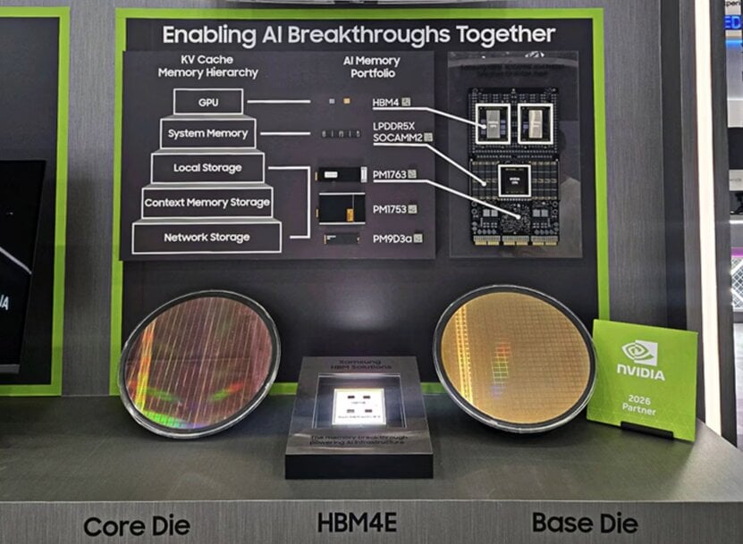
Samsung Electronics demonstrated its integrated artificial intelligence (AI) semiconductor portfolio at the COMPUTEX 2026 exhibition, which took place in Taipei, Taiwan, from June 2 to June 5, 2026. Operating under the theme "Integrated AI Semiconductor Solutions," the company presented hardware configurations spanning High Bandwidth Memory (HBM), low-power server modules, and enterprise solid-state drives (SSDs) designed for end-to-end AI system deployment. The computing architecture was displayed alongside the concurrent NVIDIA GTC Taipei conference, positioning the memory hierarchy against hyperscale AI processing workflows.
Multi-Layer Memory Hierarchy and Storage Frameworks
The exhibition showcased an end-to-end AI system architecture mapped across distinct functional processing layers:
- Accelerator Memory Layer: The newly developed HBM4E platform is designed to sit directly adjacent to the graphic processing unit (GPU) socket.
- System Memory Layer: This layer featured the SOCAMM2 server module, an LPDDR5X-based memory standard optimized for high-density, low-overhead system computing.
- Enterprise Storage Layer: The base storage tier integrated an AI-optimized enterprise SSD portfolio, including the PM1753 and PM9D3a drives, alongside the flagship PM1763 model. The PM1763 utilizes a next-generation PCIe Gen6 interface to deliver the read/write throughput and power efficiency metrics demanded by dense AI training nodes.
Jaihyuk Song, Chief Technology Officer of Samsung Electronics, stated during a media briefing on June 2, 2026, that semiconductor innovation in the AI era must transition beyond isolated memory performance. Song noted that modern infrastructure development requires system-level optimization spanning advanced lithography, high-density packaging, storage throughput, thermal mechanics, and system-level architecture. He added that the company's organizational structure as an Integrated Device Manufacturer (IDM)—with capabilities unifying memory design, foundry node fabrication, logic engineering, and advanced packaging—allows it to deploy custom silicon revisions across the full AI computing stack.
HBM4E Specifications and Heat Path Block Engineering
The core hardware introduction consisted of the HBM4E memory module, which provides a 30% capacity increase over previous-generation designs to handle large language model parameters and data-intensive compute workloads. The device architecture unifies a Core Die fabricated on a 1c nm DRAM process node with a Base Die manufactured via Samsung Foundry’s 4nm logic process. The silicon layout achieves native data transfer speeds of up to 14 Gbps per pin, features scalability to 16 Gbps, and provides a total aggregate bandwidth exceeding 4 TB/s.
To manage the high thermal flux densities generated by high-speed operations, the manufacturer introduced Heat Path Block (HPB) technology. The Die-to-Die Physical Layer (D2D PHY), which coordinates high-frequency signaling between the stacked HBM layers and the adjacent host GPU, represents a primary source of localized thermal concentration inside the Base Die. The HPB framework integrates a dedicated, low-thermal-resistance pathway directly into the die layout to accelerate heat extraction and dissipation out of the D2D PHY region. This thermal management mechanism is intended to preserve operational stability and signal integrity across high-bandwidth, high-density environments. The company is actively validating the HPB architecture on its current HBM4E designs and plans to integrate the technology as a standard specification for future HBM5 product generations.
Edited by Romila DSilva, Induportals Editor, with AI assistance.
