
electronics-journal.com
30
'26
Written on Modified on
Dual-band infrared sensor for high-resolution thermal monitoring
Fujitsu develops a dual-wavelength infrared imaging sensor to support advanced thermal detection in security, disaster monitoring, and scientific sensing applications.
www.fujitsu.com
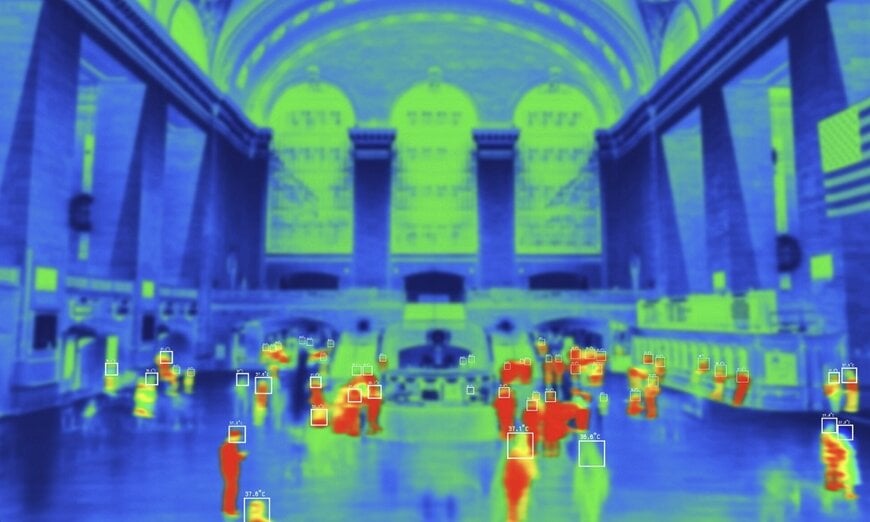
Reference image.
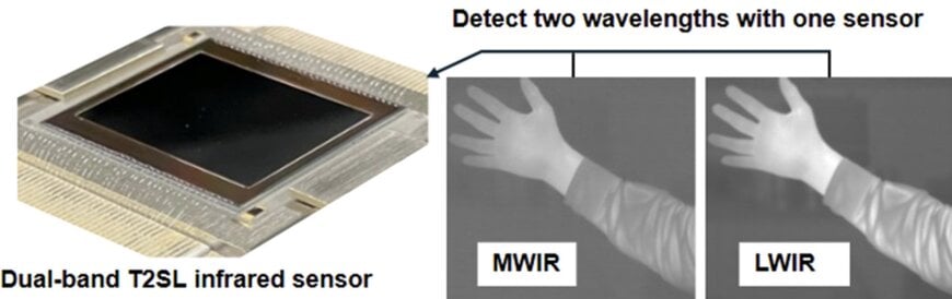
Infrared imaging systems are increasingly used in security monitoring, disaster prevention, and environmental observation where precise thermal detection and target identification are required across varying conditions. In this context, Fujitsu developed a dual-band Type-II superlattice (T2SL) infrared sensor with more than one million pixels for high-sensitivity monitoring applications.
Dual-wavelength sensing for complex monitoring environments
The developed sensor detects both mid-wavelength infrared (MWIR) and long-wavelength infrared (LWIR) radiation, allowing simultaneous multi-spectral detection within a single pixel structure. This capability improves the ability to distinguish targets from background noise compared to conventional single-wavelength infrared sensors.
The sensor can detect temperature differences of 0.05°C or less, enabling identification of small thermal variations in both daytime and nighttime monitoring scenarios. These characteristics are relevant for applications such as satellite and airborne optical sensing systems, where long-distance observation and accurate thermal discrimination are required.
Detection performance for defense and disaster prevention systems
Potential applications include monitoring systems for defense and disaster prevention, where thermal pattern analysis can support early detection of human activity, object movement, and environmental hazards. Example use cases include locating individuals during disaster response operations, identifying early-stage forest fires, and monitoring tsunami development through thermal observation.
The sensor can also support infrastructure inspection, scientific measurement systems, and analytical instrumentation by enabling visualization of temperature distribution and temporal thermal changes with high precision.
Type-II superlattice design and material engineering
The sensor design uses Type-II superlattice (T2SL) compound semiconductor structures, where multiple semiconductor layers are stacked at the nanometer scale to control material properties and detection wavelengths. This structure supports high sensitivity and enables the detection of infrared radiation with lower energy levels than visible light.
By combining semiconductor materials with large energy offsets in their band structures, the design enables stable dual-band detection while maintaining manufacturability. Process and packaging developments for the sensitive T2SL materials also enabled pixel miniaturization, allowing the sensor to achieve a resolution exceeding one megapixel and improving the ability to detect distant targets.
Research programme and product development direction
The sensor was developed as part of the “Prototype of Wide Band and High Responsivity Photo-Detectors” programme commissioned by the Acquisition Technology & Logistics Agency (ATLA) of Japan’s Ministry of Defense. Fujitsu completed delivery of the research prototype under this programme.
Edited by industrial journalist Aishwarya Mambet, with AI-assistance.
www.fujitsu.com
