
electronics-journal.com
23
'26
Written on Modified on
Efficient Thermal Path Design in Mobile Application Processor Packaging
Samsung Electronics advances mobile processor thermal architecture to support sustained performance in compact devices, integrating Heat Path Block to optimize heat dissipation for modern workloads.
semiconductor.samsung.com
Samsung Electronics has detailed a new mobile application processor (AP) package architecture that addresses thermal management limitations in conventional designs by optimizing the heat transfer path at the semiconductor package level. The architectural refinement is intended to improve thermal efficiency—a key constraint as modern mobile devices demand higher performance in increasingly slim form factors for applications such as gaming, high-performance computing, and on-device artificial intelligence.
Evolving Thermal Constraints in Mobile Packaging
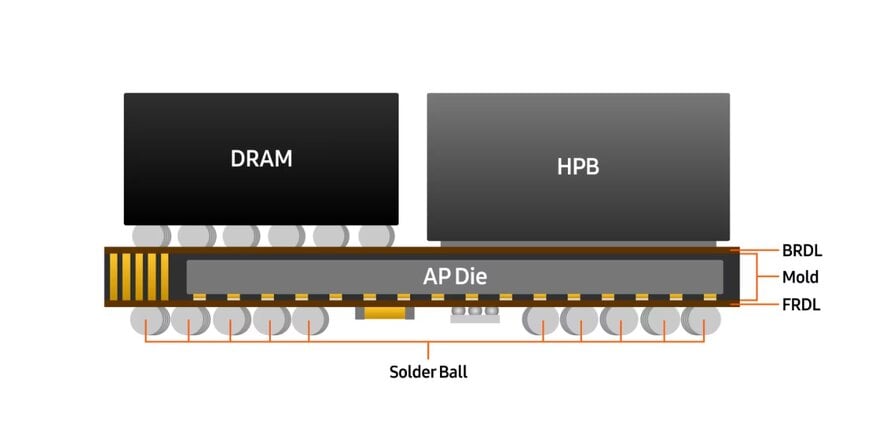
As mobile APs deliver more compute capability to support camera processing, graphics, and AI workloads, the resulting increase in power density exacerbates heat generation within space-limited smartphone environments. Effective management of thermal resistance—the opposition to heat flow from the silicon die to external cooling structures—is critical for sustaining performance without throttling under load. In conventional package-on-package (PoP) configurations, dynamic random-access memory (DRAM) is stacked directly above the AP die, creating a thermal bottleneck that limits direct heat transfer and constrains sustained performance.
Maintaining low thermal resistance is essential because elevated die temperatures force power reduction to protect device integrity, which in turn restricts the AP’s ability to operate at its designed performance level. Traditional remedies—such as improving material thermal conductivity or increasing die thickness—encounter physical and form-factor limitations as device profiles continue to thin.
Heat Path Block Integration for Optimized Thermal Efficiency
To address these structural limitations, Samsung introduced a modified package architecture employing a Heat Path Block (HPB) integrated into a fan-out wafer level package (FoWLP). By repositioning the DRAM footprint to avoid overlapping the primary heat-generating area of the AP die, and placing an HPB directly above the die, the new architecture significantly shortens the thermal pathway to external heat dissipation components. The HPB is fabricated from high-conductivity metal (copper) with thermal conductivity on the order of 400 W/m·K—approximately 500 to 1,000 times greater than typical polymer-based substrate materials—enabling more rapid outward heat transfer from the die.
Complementary to the HPB, a new thermal interface material (TIM) with enhanced conductivity and bonding reliability was introduced to maintain structural integrity while facilitating efficient heat flow. This combination aims to reduce package-level thermal resistance compared to conventional PoP packaging, with independent sources reporting up to roughly 16 per cent reduction in thermal resistance in related implementations.
Implications for Mobile Performance and Space Efficiency
This packaging refinement has direct implications for sustained processor performance in mobile systems. By lowering thermal resistance and enabling heat generated within the AP die to be transferred more directly to external cooling structures, the architecture supports more stable operation under high workload conditions without premature thermal throttling. These improvements are particularly relevant to high-performance mobile applications—including real-time graphics, machine learning inference, and intensive multi-threaded tasks—where thermal limits have historically curtailed longer-lasting performance.
The architectural shift also contributes to broader design objectives in mobile platforms. Efficient thermal pathway design can enable slimmer device profiles and greater internal space efficiency, benefiting battery capacity and overall system integration. As thermal management becomes a more central aspect of the digital supply chain for mobile APs, structural innovations such as the HPB-enhanced FoWLP help address enduring thermal barriers to performance scaling.
Technical Context and Forward Outlook
The development of this thermal architecture represents a structural evolution in AP packaging, moving beyond incremental materials improvements toward direct optimization of heat transfer paths. The HPB’s introduction in mobile AP packaging underscores the role of package-level innovations in enabling next-generation performance within constrained form factors. As device performance requirements continue to rise, thermal management at the packaging level is poised to remain a critical component in advancing mobile processor capabilities.
www.semiconductor.samsung.com
