
electronics-journal.com
13
'26
Written on Modified on
300 mm silicon photonics targets AI interconnect scaling
CEA-Leti collaborates with NcodiN to move optical interposer technology toward wafer-scale manufacturing for high-bandwidth computing and AI processor integration.
www.cea.fr
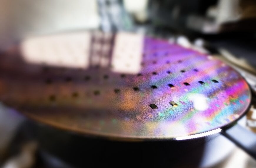
III-V semiconductor dies bonded to 300mm wafer using direct bonding and high-precision alignment. Credit: AUBERT/CEA
Optical interconnects are gaining relevance as semiconductor designers address bandwidth and energy constraints in AI computing and high-performance processors. In this context, CEA-Leti and NcodiN announced a collaboration to industrialise silicon photonics interposer technology using 300 mm wafer processes.
Optical interconnects addressing AI data movement limits
The collaboration focuses on next-generation semiconductor architectures used in AI accelerators and high-performance computing, where conventional copper interconnects increasingly limit bandwidth and power efficiency.
NcodiN is developing optical interconnect technology intended to address data transfer bottlenecks between chips and within advanced packages. The transition from copper to optical links reflects broader industry efforts to improve bandwidth density and reduce energy per transmitted bit in AI systems.
The joint work aims to move NcodiN’s proof-of-concept photonic interposer technology toward industrial 300 mm silicon photonics manufacturing, aligning development with standard semiconductor fabrication processes.
Nanoscale laser integration for dense photonic interposers
NcodiN’s NConnect optical interconnect platform integrates nanolaser technology described as significantly smaller than conventional silicon photonics light sources. The architecture is designed to support integration densities exceeding 5,000 nanolasers per square millimetre and energy efficiency around 0.1 pJ per transmitted bit.
The collaboration with CEA-Leti focuses on transferring this nanolaser technology to a 300 mm silicon photonics platform compatible with CMOS manufacturing. This step is intended to support wafer-level integration of optical interconnects for use in advanced computing devices.
Technical objectives include demonstrating compatibility with high-volume wafer processing to support cost and scalability requirements associated with AI processors and bandwidth-intensive computing platforms.
From laboratory photonics to semiconductor manufacturing
CEA-Leti’s role in the collaboration includes support for photonics integration and transfer of microelectronics research into industrial processes. Moving photonic interconnects to 300 mm CMOS-compatible fabrication is intended to allow production within existing semiconductor manufacturing infrastructure.
The partners are targeting in-package optical interconnects capable of supporting long-reach data transmission within computing systems. Such approaches are being explored as part of the broader evolution of AI hardware and semiconductor packaging, where integration density and interconnect efficiency influence overall system performance.
This development reflects ongoing efforts across the semiconductor ecosystem to introduce photonic communication technologies capable of supporting increasing data movement requirements within AI computing architectures.
www.leti-cea.com
Edited by industrial journalist, Aishwarya Mambet — AI-powered.
