
electronics-journal.com
12
'26
Written on Modified on
Multi-Die Design Frameworks for Advanced Semiconductor Systems
Samsung Foundry and Synopsys collaborate to develop integrated design flows enabling multi-die semiconductor architectures for AI, HPC, and advanced computing applications.
semiconductor.samsung.com
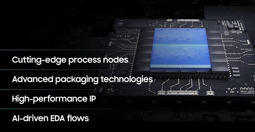
The shift from monolithic system-on-chip (SoC) designs to multi-die architectures using chiplets is increasing design complexity across semiconductor development. Samsung Foundry and Synopsys are cooperating to provide integrated design flows combining process technology, packaging, IP, and electronic design automation (EDA) tools to support advanced semiconductor systems used in AI and high-performance computing.
Context of the Cooperation
Growing compute demands from artificial intelligence and high-performance computing workloads require higher transistor density, greater memory bandwidth, and improved energy efficiency. At advanced process nodes, however, large monolithic dies present manufacturing challenges related to yield, cost, and design scalability.
Multi-die architectures address these issues by integrating multiple smaller chiplets within a single package using high-speed die-to-die interconnects and advanced packaging technologies. This approach introduces additional engineering constraints, including signal integrity, power delivery, thermal behavior, and interposer routing.
Samsung Foundry and Synopsys are collaborating to address these challenges by aligning foundry manufacturing technologies with system-level design methodologies. The cooperation combines Samsung’s process and packaging capabilities with Synopsys’ electronic design automation tools and interface IP to support complex semiconductor development.
Technical Solution and Responsibilities
The collaboration focuses on integrated design frameworks based on system-technology co-optimization (STCO), extending beyond traditional design-technology co-optimization (DTCO). Instead of optimizing individual chip blocks separately, STCO evaluates trade-offs across dies, interconnect structures, packaging, power networks, and thermal conditions at the system level.
Synopsys provides design automation platforms such as 3DIC Compiler, which supports multi-die implementation, interposer routing, signal integrity verification, and multiphysics analysis. The platform enables engineers to evaluate design options and verify power, thermal, and electrical characteristics across both dies and packaging structures.
Samsung Foundry contributes process technologies, packaging platforms, and design enablement for multi-die integration. Examples include the SF2P and SF4X process nodes and advanced packaging solutions such as 2.5D Cube-S interposer technology.
Deployment and Implementation
Joint development work has been applied to several semiconductor design projects involving multi-die integration. One implementation involved a customer tape-out using the SF2P process combined with Cube-S packaging and automated multi-die implementation through the Synopsys 3DIC Compiler. According to project data, automated design workflows reduced design turnaround time by approximately 50% while improving signal integrity metrics by about 6%.
Another collaboration validated a 2.5D interposer architecture integrating system-on-chip components, DRAM, and next-generation HBM4 memory interfaces. Automated routing across the interposer was used to evaluate signal integrity and packaging feasibility.
The partners also completed a tape-out using Samsung’s SF4X process to validate UCIe (Universal Chiplet Interconnect Express) interface IP operating at 32 Gbit/s, demonstrating readiness for open chiplet interconnect standards.
Applications and Use Cases
The integrated design frameworks target semiconductor products used in AI accelerators, high-performance computing platforms, automotive electronics, and edge computing systems. These applications require high bandwidth memory integration, scalable compute architectures, and advanced packaging technologies.
Multi-die design methodologies supported by the collaboration enable engineers to analyze thermal, electrical, and mechanical interactions across chiplets and packaging structures during early design phases, improving predictability and reducing integration risks.
Results and Expected Impact
By combining foundry process capabilities with AI-assisted EDA workflows, the cooperation supports faster exploration of design alternatives and more efficient system-level optimization. Automated analysis of power delivery, thermal behavior, and signal integrity allows semiconductor developers to manage the increasing complexity of multi-die systems.
As chiplet-based architectures expand across multiple industries, integrated design environments linking manufacturing technologies with digital semiconductor design infrastructure are expected to play an important role in enabling scalable system development.
Edited by an industrial journalist, Sucithra Mani — AI-powered.
www.samsung.com
