
electronics-journal.com
11
'26
Written on Modified on
Nexperia Introduces New Low Voltage GaN FETs For Power Conversion
New high efficiency devices deliver record low on state resistance to support artificial intelligence datacentres humanoid robotics renewable energy and advanced power conversion system architectures.
www.nexperia.com
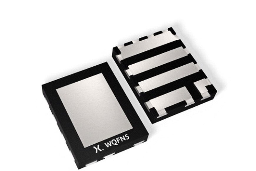
Modern power conversion architectures face severe efficiency, thermal dissipation, and space constraints as compute-intensive AI infrastructure and compact industrial robotics demand unprecedented current delivery. Meeting these requirements requires wide-bandgap semiconductor solutions that minimize parasitic losses and overcome the physical switching limits inherent in legacy silicon MOSFETs.
Overcoming Switching and Conduction Losses in Power Conversion
Power architects designing intermediate bus converters, synchronous rectification stages, and high-frequency inverters continuously balance conduction losses against switching losses. Traditional silicon power stages operating at high currents require larger die areas to decrease on-state resistance, which inversely increases gate charge and output capacitance, capping practical switching frequencies and demanding bulky passive components.
To address this technical hurdle, wide-bandgap gallium nitride technology provides significantly lower figures of merit, specifically the products of on-state resistance and gate charge, as well as on-state resistance and output charge. This reduction in parasitic charge enables power engineers to operate at elevated switching frequencies without incurring prohibitive switching losses, substantially reducing the physical footprint of inductors and capacitors in modern power electronics.
Technical Architecture and Figures of Merit
Nexperia structured this semiconductor expansion across a voltage range of 18 V to 200 V, utilizing GaN device physics to achieve sub-milliohm on-state resistance within printed circuit board footprints as compact as 10 mm². Low parasitic charges decrease switching transitions, supporting precise dead-time control and full 100 percent duty-cycle operation where required.
Thermal management is handled through surface-mount packaging equipped with exposed pads engineered for top-side cooling. The family includes 3.3 mm by 3.3 mm PQFN and 3 mm by 5 mm PQFN outlines. By routing heat dissipation directly through the top surface rather than saturating the underlying circuit board, these packages assist engineers in optimizing PCB thermal design and lowering overall junction temperatures under continuous high-current operation.
System Integration in DC-DC Conversion and Motion Control
The portfolio targets specific stages within multi-stage power delivery networks and dynamic drive topologies:
In 48 V power distribution networks common to computing and telecommunications infrastructure, the medium-voltage 100 V to 200 V components serve in isolated primary-side and secondary-side stages, including full-bridge and half-bridge LLC resonant topologies. They also function within non-isolated step-down converters that drop intermediate distribution buses down to sub-rails.
For point-of-load architectures, low-voltage devices rated from 18 V to 40 V provide secondary-side synchronous rectification, supporting efficient step-down conversion from 12 V intermediate rails directly to core voltages below 1 V.
In precision motion control, such as three-phase brushless DC and permanent-magnet synchronous motor drives, the low on-resistance combined with rapid switching dynamics allows drive stages to execute high-frequency pulse-width modulation. This enhances phase current tracking and overall inverter operating efficiency in space-constrained applications like humanoid robotic joints and cordless power equipment.
Technical Specifications and Portfolio Availability
The product rollout comprises eight devices across discrete voltage tiers:
The flagship 100 V device, designated GANE0R8-100QTM, specifies a typical on-state resistance of 0.75 mΩ housed in a 3 mm by 5 mm PQFN package.
Five complementary devices covering ratings between 25 V and 200 V deliver on-state resistance values down to 0.37 mΩ.
Two forthcoming portfolio additions, including the 18 V GANE0R3-015QTL with a typical on-state resistance of 0.32 mΩ in a 3.3 mm by 3.3 mm package, are scheduled for release in the first quarter of 2027.
Engineering Strategy for Power Distribution Networks
Andrea Bricconi, Vice President and Head of the GaN Product Group at Nexperia, noted that expanding wide-bandgap portfolios provides the foundational power stages required by systems that demand increased power density and operational efficiency across AI installations and robotics.
Roberto Crisafulli, Director of GaN Marketing and Applications at Nexperia, outlined the architectural context, stating that multi-stage power distribution networks in compute facilities are transitioning across step-down hierarchies from 800 VDC to 48 VDC, 12 VDC, and 6 VDC, requiring modular low- and medium-voltage semiconductor building blocks capable of scaling within stacked topologies.
Additional Context
This section details technical specifications and competitive benchmarking not included in the original product announcement.
The shift toward gallium nitride in low-to-medium voltage domains (below 200 V) represents an ongoing technological evolution within enterprise and hyperscale facilities, largely driven by open standards organizations such as the Open Compute Project (OCP). OCP standards have accelerated the global deployment of 48 V server racks, replacing traditional 12 V multi-drop busbars to mitigate resistive I²R transmission losses by a factor of 16 for a given power level.
Within this 48 V conversion hierarchy, standard benchmark silicon MOSFETs (such as OptiMOS or similar trench technologies) generally exhibit typical RDS(on) × QG figures of merit exceeding 40 to 60 mΩ·nC in the 80 V to 100 V rating class. In contrast, lateral GaN high-electron-mobility transistor (HEMT) architectures typically operate with figures of merit below 15 to 25 mΩ·nC, alongside zero reverse-recovery charge (Qrr = 0). This eliminates reverse-recovery losses in synchronous rectification and hard-switched bridges.
Direct industry benchmarks for 100 V surface-mount GaN components include devices such as the EPC2065 (EPC) and GS-065-004 (GaN Systems / Infineon). While chip-scale packaging (wafer-level CSP/BGA) offers minimal package inductance, PQFN packages featuring exposed top-side cooling provide distinct manufacturing and mechanical reliability advantages in industrial and automotive-adjacent assembly lines, balancing automated optical inspection compatibility with direct thermal attachment to secondary heatsinks.
Edited by Evgeny Churilov, Induportals Media - Adapted by AI.
www.nexperia.com
