
electronics-journal.com
30
'26
Written on Modified on
NVIDIA Speeds Up Design of Next-Generation CPUs and GPUs
The Vera CPU is speeding up next-generation NVIDIA chip designs, and early testing shows up to 1.5x higher performance on key verification and simulation workloads.
www.nvidia.com
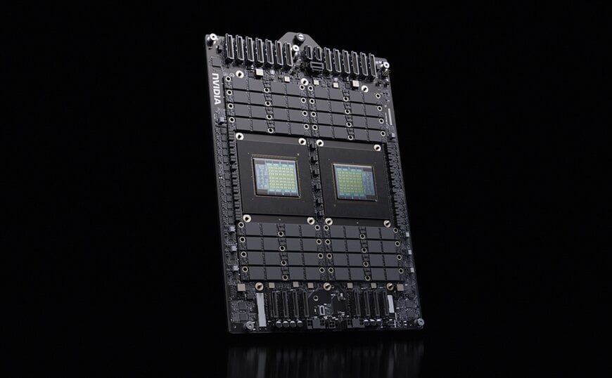
NVIDIA is collaborating with Cadence and Synopsys to optimize electronic design automation (EDA) applications for the NVIDIA Vera CPU, while deploying the processor across its internal chip design workflows. The integration aims to accelerate logic simulation, formal verification, and digital implementation for next-generation CPU and GPU development.
Collaboration and Initial Performance Benchmark Results
Simulation, verification, and implementation technologies play a central role in semiconductor development. Before a chip reaches manufacturing, engineering teams validate behavior, identify corner cases, and refine designs through thousands of iterations.
While graphics processing units (GPUs) and artificial intelligence (AI) have accelerated various aspects of chip design, several critical EDA workloads remain dependent on CPU performance. Logic simulation, formal verification, and portions of digital implementation rely on fast individual core performance, memory system efficiency, and overall compute throughput.
NVIDIA's initial testing evaluated leading EDA software platforms. Testing included Cadence Jasper, a formal verification platform utilizing smart proof technology and machine learning, and Synopsys VCS, a high-performance functional verification solution for simulating and validating complex chip designs prior to fabrication. Using identical core counts, both applications demonstrated up to 1.5x higher performance on selected workloads. Beyond benchmark testing, NVIDIA is collaborating with both companies on application profiling, software optimization, and system-level tuning to improve engineering productivity across additional workflows over time.
Processor Microarchitecture and Design Deployment
NVIDIA is deploying Vera throughout the EDA workflows used to create future NVIDIA processors. Vera combines 88 custom NVIDIA Olympus CPU cores with an LPDDR5X memory subsystem and second-generation NVIDIA Scalable Coherent Fabric designed to deliver per-core performance, high memory bandwidth, and low latency for engineering applications.
These architectural capabilities support workloads that combine latency-sensitive execution tasks with large-scale regression testing across compute farms. Faster execution shortens individual verification runs, while higher throughput enables engineers to evaluate more design alternatives within the same development window.
Register-Transfer Level Validation and Future Roadmap
After defining a processor’s architecture and microarchitecture, engineers describe its behavior at the register-transfer level (RTL). Interconnected workflows spanning logic simulation, formal verification, regression testing, and digital implementation transform that design into manufacturable silicon.
Improvements in verification throughput allow organizations to identify potential issues earlier in the cycle, reducing downstream design iterations. Looking ahead, NVIDIA plans to follow Vera with the next-generation Rosa CPU, powered by the NVIDIA Rigel core, while continuing to optimize leading EDA applications across its CPU product roadmap.
Additional Context
This section details technical specifications not included in the original news release.
Electronic Design Automation (EDA) software provides computer-aided engineering tools for logical modeling, physical layout, functional verification, and parasitic extraction in semiconductor design. Formal verification, implemented in tools like Cadence Jasper, uses mathematical proof techniques rather than discrete test vectors to exhaustively verify that a register-transfer level (RTL) model satisfies structural and behavioral assertions under all operating conditions.
Logic simulation, as executed by Synopsys VCS, compiles hardware description languages (such as SystemVerilog, Verilog, or VHDL) into binary executables to simulate event-driven signal propagation across millions of gate-level or RTL nodes.
Monolithic CPU die designs paired with on-die interconnect fabrics, such as coherent ring or mesh networks, eliminate the inter-die routing delays and packet serialization overhead associated with multi-chiplet topologies. Low-power double data rate (LPDDR5X) memory architectures in server environments utilize wide, multi-channel physical interfaces to deliver high memory bandwidth density while maintaining lower power consumption per gigabyte per second compared to conventional registered dual in-line memory modules (RDIMMs).
Edited by Romila DSilva, Induportals Editor, with AI assistance.
www.nvidia.com
