
electronics-journal.com
01
'26
Written on Modified on
Keysight and WIN Semiconductors Launch Joint GaN MMIC Workflow
Keysight Technologies and WIN Semiconductors connect on-chip simulation and evaluation board design to enable first-pass GaN MMIC tapeout success.
www.keysight.com
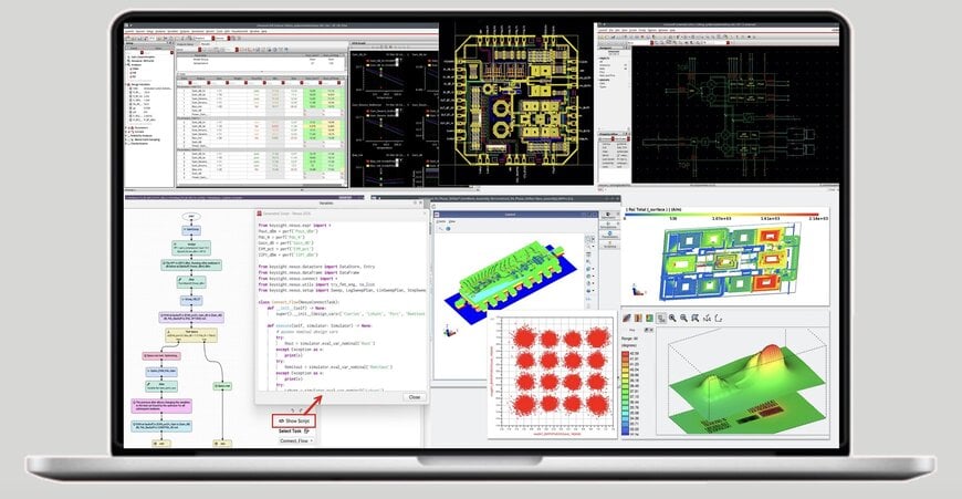
Keysight Technologies, Inc. and WIN Semiconductors Corp. have introduced a joint Monolithic Microwave Integrated Circuit (MMIC) design workflow to enable Gallium Nitride (GaN) MMIC design houses to achieve first-pass tapeout success. The environment integrates on-chip simulation, 3D layout verification, and off-chip evaluation board design for hardware applications spanning 5G base stations, Wi-Fi access points, satellite payloads, and defense radar systems.
Context of the Cooperation
A failed semiconductor tapeout can result in weeks lost to successive foundry respins, introducing significant schedule risks for design components. Furthermore, MMIC customers typically require performance validation on physical evaluation boards—comprising the MMIC, packaging, printed circuit board (PCB), and test connectors—before finalizing purchase commitments. With the global GaN radio frequency (RF) device market projected to expand to $2.77 billion by 2031, design houses face the challenge of proving complete system performance to capture market share. To address the engineering complexities of simultaneous on-chip and off-chip optimization, cooperation was established to link Keysight's simulation software tools with WIN Semiconductors’ specialized foundry process frameworks.
Technical Solution and Responsibilities
The technical solution consists of an integrated design workflow that automates the full sequence of simulation, optimization, and verification steps required to sign off on an MMIC design before foundry fabrication. Responsibilities are divided between the partners to align design simulation with foundry manufacturing constraints:
- WIN Semiconductors provides its latest NP 120P GaN Process Design Kit (PDK), which delivers the underlying process models and layout rules.
- Keysight Technologies integrates these process models within its Advanced Design System (ADS) and RF Circuit Simulation Professional software environments.
At a system level, the workflow connects on-chip multi-domain simulation, 3D layout with verifications, and off-chip MMIC evaluation board design into a single environment. This unified architecture allows engineers to design and optimize the on-chip components alongside the physical packaging, PCB, and test connectors concurrently, ensuring that the entire setup meets performance specifications when verified with test equipment.
Deployment or Implementation
The joint design workflow is structured for deployment by engineering design houses developing high-frequency components. By embedding the NP 120P GaN Process Design Kit directly within the Keysight ADS ecosystem, the automated pipeline ensures that no critical verification steps are skipped before the final design is submitted to the foundry. The implementation framework allows developers to validate performance parameters across both on-chip and off-chip layers simultaneously, establishing a streamlined process from initial layout to first-pass fabrication success.
Edited by Romila DSilva, Induportals Editor, with AI assistance.
