
electronics-journal.com
29
'26
Written on Modified on
Integrating semiconductor electronic design automation software for advanced process technologies
Siemens and Samsung Foundry cooperate to qualify digital infrastructure for next-generation semiconductor manufacturing nodes.
www.sw.siemens.com
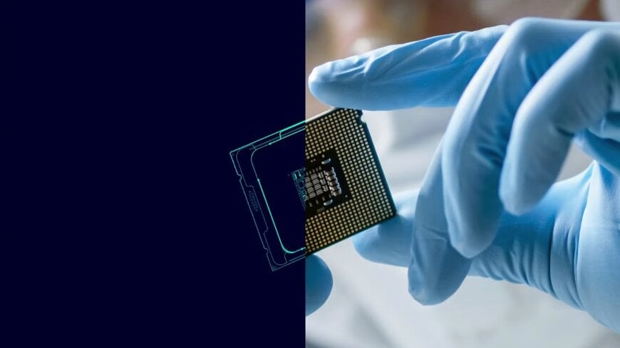
Siemens and Samsung Foundry have expanded their technical cooperation to qualify electronic design automation software across advanced semiconductor manufacturing nodes. This joint initiative integrates software tools into manufacturing workflows to support the design, verification, simulation, and manufacturing of integrated circuits for the global fabless ecosystem.
The technical challenge stems from the escalating complexity of sub-5nm semiconductor designs, where physical effects like electromigration, voltage drop, and curvilinear geometries require precise engineering validation. To address these integration complexities, the companies align software functionality directly with manufacturing process parameters, ensuring design verification and reliability prior to fabrication.
Physical Verification and Layout Optimization
The integration qualifies the Calibre nmPlatform software for physical validation within Samsung Foundry processes. To improve power-grid robustness, the implementation incorporates automated layout enhancements via Calibre DesignEnhancer software for 2nm process technologies. This automation mitigates electromigration and voltage drop by executing design-rule-checking-compliant layout modifications. Additionally, the cooperation extends to photonic integrated circuit verification, establishing equation-based design rule checking and curvilinear layout-versus-schematic verification to manage non-linear geometries.
Advanced Packaging and 3D Integration
For high-density packaging architectures, the integration utilizes specialized software tools to support the 2.3D Cube-E package platform. The implementation utilizes Innovator3D IC Integrator for early-stage project floorplanning and netlist generation for complex systems exceeding two million pins. Physical verification of these multi-die assemblies is completed through Calibre 3DStack to verify architectural integrity across 2.5D and 3D implementations.
Simulation, Yield Analysis, and Digital Implementation
The scope of the technical alignment includes the following domains:
- Analog and RF Verification: The Solido Simulation Suite is qualified for spice-accurate verification, including automotive applications on 4nm and 2nm nodes. The system utilizes the Open Model Interface to perform aging and reliability analysis across process technologies ranging from 14nm down to 2nm.
- Design-for-Test (DFT): The Tessent portfolio introduces a high-resolution chain diagnosis reference flow. This layout-aware and cell-aware methodology accelerates physical failure analysis and improves failure isolation during yield analysis.
- Digital Implementation: The Aprisa software is certified for advanced process nodes to optimize power, performance, and area metrics, accelerating design closure.
