
electronics-journal.com
10
'26
Written on Modified on
Siemens accelerates AI chip verification with NVIDIA
FPGA-based prototyping enables trillion-cycle pre-silicon validation, addressing scalability challenges in complex AI/ML system-on-chip development.
www.siemens.com
Semiconductor design, AI/ML system-on-chip (SoC) development, and electronic system verification increasingly require scalable validation methods to handle growing architectural and software complexity. In this context, Siemens, in collaboration with NVIDIA, has advanced hardware-assisted verification capabilities to support trillion-cycle validation at the pre-silicon stage.
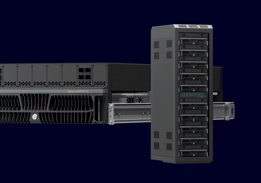
The development is based on Siemens’ Veloce proFPGA CS platform, combined with NVIDIA’s performance-optimized chip architectures, enabling designers to execute and capture tens of trillions of verification cycles within a few days.
Scaling verification beyond traditional limits
As AI/ML SoCs increase in complexity, verification workloads have expanded significantly, driven by both hardware architecture and software stack requirements. Conventional verification approaches such as simulation and emulation typically handle millions to a few billion cycles within practical timeframes, creating bottlenecks in development.
The use of FPGA-based prototyping systems allows these workloads to be executed much faster by running designs in hardware rather than purely in software models. With the Veloce proFPGA CS system, this approach scales to trillions of cycles, enabling validation scenarios that were previously impractical.
FPGA-based prototyping for AI/ML systems
The Veloce proFPGA CS platform is designed to provide a scalable and flexible hardware architecture for both single-FPGA IP validation and multi-billion-gate chiplet designs. By integrating NVIDIA’s chip architectures, the system supports large-scale workload execution, allowing engineers to validate functional behaviour and system performance before silicon fabrication.
This capability is particularly relevant for AI/ML applications, where workloads are data-intensive and require extensive validation to ensure reliability and performance under real-world conditions.
Impact on development timelines and reliability
Running trillions of verification cycles in a short period enables earlier detection of design issues, reducing the risk of costly redesigns after fabrication. This contributes to shorter time-to-market while maintaining reliability standards required for advanced semiconductor devices.
According to NVIDIA, the ability to validate large workloads at scale provides confidence in next-generation AI architectures, particularly as computing systems continue to evolve in complexity.
Applications in advanced semiconductor design
This verification approach is applicable across a range of semiconductor applications, including AI accelerators, data center processors, and high-performance computing systems. In these domains, ensuring correct operation under extensive workloads is essential before committing to production.
By combining FPGA-based prototyping with scalable verification infrastructure, the collaboration between Siemens and NVIDIA addresses a key industry challenge: validating increasingly complex designs within realistic development timelines.
Edited by Natania Lyngdoh, Induportals Editor — Adapted by AI.
www.siemens.com
