
electronics-journal.com
25
'26
Written on Modified on
Automotive MOSFETs in compact wettable flank packages
Toshiba introduces DFN2020B package devices to support miniaturized automotive electronics with improved inspection capability and solder joint reliability.
www.global.toshiba
Automotive electronic systems continue to require higher component density while maintaining reliability and manufacturability under automotive qualification standards. In this context, Toshiba Electronics Europe introduced five automotive MOSFETs in a DFN2020B package featuring wettable sidewalls to support miniaturization and automated inspection processes.
Package design supporting automated manufacturing inspection
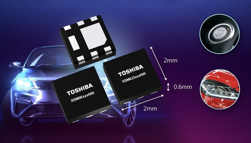
The newly introduced N-channel devices (XSM6K361NW, XSM6K519NW, XSM6K376NW, XSM6K336NW) and the P-channel XSM6J372NW MOSFET use the DFN2020B(WF) package, which incorporates a wettable flank structure to improve solder joint inspection during assembly.
The package design improves solder wettability compared with Toshiba’s UDFN6B package and increases solder fillet visibility, enabling automated optical inspection (AOI) systems to verify solder joint quality more reliably. Mechanical testing also showed approximately 23 % higher solder joint shear strength compared with the SOT-23F package, supporting improved assembly robustness.
Size reduction for dense automotive electronics layouts
With typical dimensions of 2.0 mm × 2.0 mm × 0.6 mm, the DFN2020B(WF) package reduces mounting area by approximately 43 % and package height by approximately 25 % compared with the SOT-23F package (2.4 mm × 2.9 mm × 0.8 mm).
Such reductions support the continued miniaturization of automotive electronic modules where PCB space constraints remain a key design factor, particularly in distributed control architectures.
Power dissipation in compact MOSFET formats
Despite the reduced package size, the devices maintain relatively high power dissipation capability. For example, the XSM6K361NW supports a maximum power dissipation of 1.84 W, compared with 1.2 W for the SSM3K361R in the SOT-23F package.
This allows the components to support applications requiring compact high-power switching devices, including DC-DC converters in electronic control units (ECUs) and load switching circuits in LED lighting systems.
Automotive qualification and roadmap considerations
The MOSFETs comply with AEC-Q101 automotive reliability testing requirements and align with the Production Part Approval Process (PPAP) defined under the IATF 16949 automotive quality management framework.
Toshiba indicated plans to further expand its MOSFET portfolio based on the DFN2020B(WF) package, including future 2-in-1 MOSFET designs intended for automotive applications.
Edited by industrial journalist Aishwarya Mambet, with AI-assistance.
www.toshiba.com
