
electronics-journal.com
25
'26
Written on Modified on
Bidirectional GaN switch for high-voltage conversion
Renesas Electronics develops a depletion-mode GaN device enabling simpler converter architectures for solar, EV charging and data-center power systems.
www.renesas.com
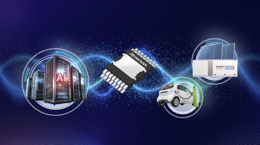
Efficiency and component reduction remain key design targets in power electronics used in renewable energy, electric mobility, and digital power infrastructure. In this context, Renesas Electronics Corporation introduced a high-voltage bidirectional GaN switch designed to enable simpler single-stage converter topologies.
Reducing switch count in converter topologies
Most high-power converter designs rely on unidirectional silicon or silicon carbide (SiC) switches that only block current in one direction in the off state. This typically necessitates multi-stage conversion architectures with multiple bridge circuits.
Solar microinverters illustrate this constraint. A typical design uses a four-switch full bridge for DC-DC conversion followed by another stage for DC-AC conversion. Even in single-stage designs, engineers often compensate by connecting conventional switches back-to-back, increasing device count and switching losses.
The bidirectional GaN design integrates reverse blocking capability into a single device, allowing single-stage conversion with fewer switches. In a representative solar microinverter implementation, two Renesas SuperGaN® bidirectional devices can replace larger switch arrangements while removing intermediate DC-link capacitors.
Switching behaviour and efficiency impact
GaN switching devices support higher switching frequencies due to low stored charge and fast transition behaviour, supporting higher power density designs.
Testing in a single-stage solar microinverter configuration showed conversion efficiency exceeding 97.5 %, supported by the elimination of back-to-back device configurations and slower silicon switches.
This makes the technology applicable in systems such as AI data-center power supplies, onboard EV chargers, and distributed solar converters where switching losses directly influence thermal design and system efficiency.
GaN device architecture and gate drive compatibility
The TP65B110HRU integrates a high-voltage depletion-mode GaN device with two low-voltage silicon MOSFETs. The design features a typical 3 V threshold voltage, ±20 V gate tolerance and integrated body diodes supporting reverse conduction.
Unlike enhancement-mode bidirectional GaN devices, the switch operates with standard gate drivers without requiring negative gate bias. This reduces gate drive complexity and supports stable switching under both hard- and soft-switching conditions.
For hard-switched topologies such as Vienna rectifiers, the device supports dv/dt capability above 100 V/ns, enabling fast transitions with limited ringing and switching delays.
Electrical parameters and integration details
The device supports ±650 V continuous AC/DC operation and ±800 V transient voltages, with a typical RDS(on) of 110 mΩ at 25 °C.
Additional specifications include dv/dt immunity above 100 V/ns, a 1.8 V freewheeling diode voltage drop, and a TOLT top-side cooled package with an industry-standard pinout to support thermal design and PCB compatibility.
Evaluation and reference designs
An evaluation kit (RTDACHB0000RS-MS-1) supports testing across different gate drive configurations, AC zero-crossing detection, and zero-voltage switching (ZVS) implementation.
The device is also part of Renesas system reference designs, including a 500 W solar microinverter and three-phase Vienna rectifier platforms combining compatible controllers, gate drivers and power management ICs to reduce design complexity and integration risk.
Edited by industrial journalist Aishwarya Mambet, with AI-assistance.
www.renesas.com
