
electronics-journal.com
25
'26
Written on Modified on
Keysight Technologies Launches Breakthrough EOE Simulation Solution
The unified workflow enables engineers to simulate complete electrical-optical-electrical signal chains, catching cross-domain issues and accelerating design tradeoffs for next-generation AI infrastructure.
www.keysight.com
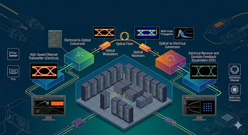
Keysight Technologies, Inc. has developed a co-simulation environment that integrates electrical and optical signal chains into a single workflow to accelerate the development of next-generation data center infrastructure.
Co-Simulation Architecture for Mixed Domain Signal Integrity
The integration of Advanced Design System 2026 handles a critical shift in high-performance computing and artificial intelligence infrastructure. As data rates scale, traditional infrastructure relies on optical links to connect central processing units, graphics processing units, and high-speed serializer/deserializer interfaces. Industry projections indicate that by 2029, 87% of hyperscale optical transceivers will operate at speeds of 800 gigabits per second (Gbps) or higher, with roadmaps extending to 1.6 terabits per second (Tbps) and 3.2 Tbps.
Legacy validation methodologies require engineering teams to simulate electrical channels and optical components in isolated software tools, subsequently stitching the disparate data sets together manually. This disconnected approach frequently fails to capture cross-domain electro-optical interactions, masking signal integrity faults until physical prototyping. The updated electronic design automation platform bridges these domains by linking electrical channel simulators with optical envelope simulators, allowing technical teams to execute end-to-end electrical-optical-electrical simulation before physical hardware manufacturing.
Bidirectional Waveguide Modeling and Nonlinear Effects
Operating at speeds such as 800Gbps and 1.6Tbps necessitates advanced modulation schemes and multi-lane topologies, which introduce complex physical phenomena. The software architecture incorporates full-duplex optical simulation to capture concurrent forward and backward signal propagation within a single optical channel. This bidirectional modeling capability represents a shift from idealized, unidirectional optical abstractions by accounting for reflections and backscattering as they occur in physical waveguides.
Furthermore, high-speed optical links increasingly rely on wavelength division multiplexing to scale bandwidth over a single fiber. The electrical-optical-electrical simulation framework includes dedicated support for wavelength division multiplexing, allowing engineers to analyze how optical nonlinearities affect performance across multiple simultaneous wavelengths on the same waveguide. The system models modulator bias-dependent variations and large-signal nonlinearities alongside multi-domain noise distributions, providing an accurate assessment of system-level bit error rates and eye diagram metrics.
Component Level Integration and Process Design Kit Support
The unified workflow spans from high-level system architecture down to granular device optimization. The platform achieves this depth by combining a high-speed digital design workflow with dedicated photonics design tools, incorporating component-level simulation through integrated photonics solvers.
Circuit-level accuracy is maintained through native Process Design Kit support from silicon photonics foundries. By tying foundry-validated component models directly to the system simulator, the software eliminates the abstraction gaps between physical photonic integrated circuit behavior and macro-level link performance.
Additional Context
This section details technical specifications and competitive benchmarking not included in the original product announcement.
The transition to multi-domain co-simulation addresses a highly competitive landscape in the electronic design automation industry. Traditionally, engineers have had to choose between specialized optical simulators, like Ansys Lumerical or Synopsys OptSim, and robust electrical channel simulators, such as those within Cadence Sigrity or Mentor Graphics platforms. For example, while Ansys Lumerical offers deep photonic integrated circuit and device-level analysis, integrating its optical S-parameter outputs into electrical channel simulators like Cadence Virtuoso often requires manual data formatting and loses dynamic, time-domain cross-talk analytics.
Keysight's integration of its RSoft component technology directly with the Advanced Design System frequency- and time-domain solvers establishes a competitive benchmark by natively unifying the electrical transient and optical envelope domains. Compared to iterative file-exporting workflows, a tight algorithmic coupling allows the simulator to calculate simultaneous electrical-optical-electrical noise figures and inter-channel cross-talk across multiple modulated lasers in a single matrix inversion, reducing total simulation time for complex 1.6Tbps links and mitigating human error in manual multi-tool scripting.
Edited by Evgeny Churilov, Induportals Media - Adapted by AI.
www.keysight.com
