
electronics-journal.com
20
'26
Written on Modified on
High-performance 3nm system-on-chip technologies for automotive multi-domain control units
Renesas Electronics Corporation has developed advanced semiconductor technologies to enable secure, high-speed data processing and chiplet scalability for the next generation of software-defined vehicles.
www.renesas.com
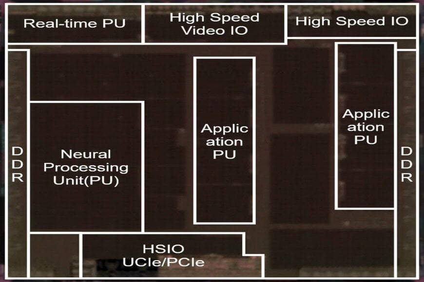
As the automotive industry transitions toward centralized computing, system-on-chip (SoC) designs must manage multiple high-intensity applications simultaneously while maintaining strict safety standards. Renesas has introduced a suite of technologies, including a functional safety-compliant chiplet architecture and 3nm AI processing optimizations, to address the increasing complexity of the automotive data ecosystem. These innovations provide the hardware foundation for multi-domain electronic control units (ECUs) that integrate advanced driver assistance systems (ADAS), infotainment, and gateway functions on a single platform.
Chiplet architecture for functional safety and scalability
The transition to software-defined vehicles (SDVs) requires SoCs that can scale performance without compromising safety. Renesas has developed a proprietary architecture that supports ASIL D functional safety requirements within a chiplet configuration. By utilizing the Universal Chiplet Interconnect Express (UCIe) standard, the system enables modular expansion through die-to-die connectivity.
To ensure "Freedom from Interference" (FFI) when multiple applications run concurrently, the architecture incorporates a RegionID mechanism. This technology maps specific IDs into the physical address space and encodes them into the UCIe region, allowing the memory management unit (MMU) and real-time cores to control access across chiplets securely. Testing confirmed that this interface maintains a transmission speed of 51.2 GB/s, ensuring that the high-bandwidth requirements of processors to memory buses are met even in distributed multi-die systems.
Advanced AI processing and 3nm manufacturing
To meet the performance demands of automated driving and cockpit intelligence, the new technologies utilize a 3nm process node. This advanced manufacturing reduces power consumption by 30 to 35 percent compared to 5nm alternatives, a critical factor for thermal management in a dense digital supply chain.
The design features a redesigned clock architecture to support larger Neural Processing Units (NPUs). As NPUs expand in area to handle complex AI workloads, clock latency between shared sources and individual circuits typically increases. Renesas addressed this by replacing module-level clock pulse generators (CPGs) with mini-CPGs (mCPGs) at the sub-module level. To maintain the "zero-defect" quality required for automotive applications, test circuits are integrated into this hierarchical architecture, synchronizing user and test clocks under a single source in test mode to allow for unified phase adjustment.
These technologies are implemented in the R-Car X5H SoC, which is designed to consolidate various vehicle functions that previously required separate hardware. Technical use cases include:
- Centralized Computing: Integrating 32 Arm Cortex-A720AE cores and six Cortex-R52 dual-lockstep cores to handle both application-level tasks and safety-critical real-time processing.
- AI Acceleration: Delivering up to 400 TOPS (Tera Operations Per Second) of performance for sensor fusion and generative AI interactions, with the ability to scale further via chiplet extensions.
- Hardware Isolation: Utilizing hardware-based isolation to separate safety-critical functions, such as brake-by-wire, from non-critical infotainment systems, preventing software faults in one domain from impacting others.
