
electronics-journal.com
13
'26
Written on Modified on
Nexperia Launches New 750 V Silicon Carbide Trench MOSFET Family
New wide bandgap devices deliver low switching losses, temperature stability, and TOLL packaging options to optimize power density across automotive, industrial, and AI infrastructure.
www.nexperia.com
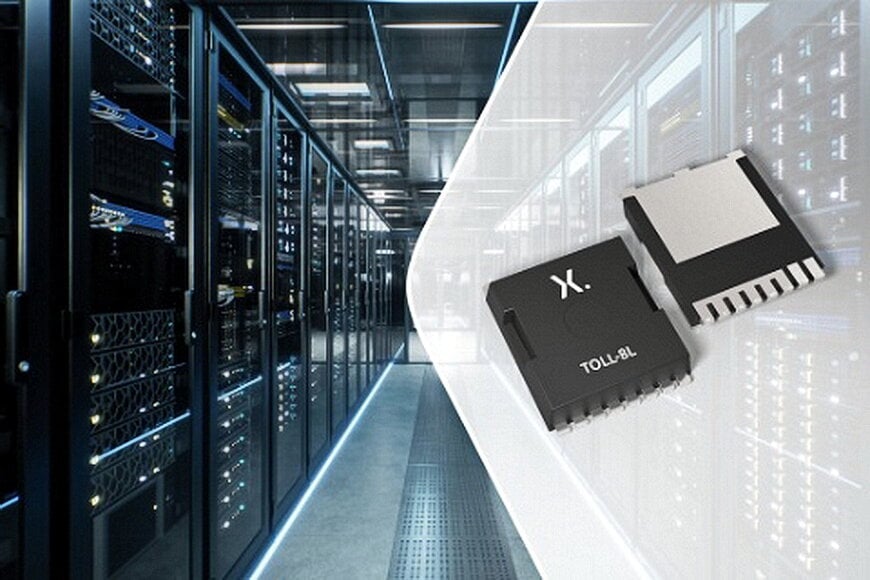
Modern power conversion architectures across renewable energy, electric vehicles, industrial automation, and artificial intelligence data centers face increasing demands for higher power density, greater conversion efficiency, and tighter thermal management. As system bus voltages rise and switching frequencies increase to shrink passive magnetic components, traditional silicon power semiconductors encounter fundamental material limits in switching speed and breakdown voltage. To address these engineering constraints, Nexperia has introduced a family of 750 V silicon carbide (SiC) trench MOSFETs, expanding its wide bandgap portfolio with industrial and AEC-Q101-qualified automotive devices available in multiple package formats, including the surface-mount TOLL (TO-Leadless) package.
Addressing Voltage Headroom and Thermal Stability in Power Conversion
Designing high-power converters for 400 V to 500 V DC bus architectures — such as automotive onboard chargers, DC-DC converters, and solar string inverters — requires sufficient voltage margin to withstand inductive voltage overshoots and transient surges during fast switching events. While 650 V devices have historically served these bus voltages, engineers increasingly specify 750 V ratings to provide an extra 100 V of blocking voltage headroom without stepping up to higher-resistance 1200 V components.
In real-world power stages, semiconductor junction temperatures fluctuate significantly under varying load profiles. A primary challenge with conventional MOSFETs is the steep rise in drain-source on-state resistance (RDS(on)) as temperature increases, which elevates conduction losses and complicates thermal design. Nexperia’s 750 V SiC trench MOSFETs are engineered to exhibit temperature-stable RDS(on) characteristics across their operating temperature range, alongside low switching losses and temperature-stable turn-off behavior. This thermal stability ensures predictable electrical performance under medium and high load conditions, allowing system architects to reduce heatsink dimensions and simplify cooling infrastructure.
Trench Gate Architecture and TOLL Package Integration
Unlike planar MOSFET structures, where the conductive channel forms horizontally along the semiconductor surface, a trench MOSFET places the gate electrode vertically inside a trench etched into the silicon carbide substrate. This vertical channel geometry increases cell density, reduces specific on-resistance, and lowers gate-to-drain capacitance, enabling faster switching transitions and lower dynamic losses.
To support high-frequency hard-switching topologies — such as totem-pole power factor correction (PFC) stages and bidirectional DC-DC converters — the devices incorporate a robust intrinsic body diode capable of handling reverse recovery stress during dead-time intervals.
A notable structural addition to Nexperia’s SiC lineup is the TOLL surface-mount package. High-speed SiC switching can induce parasitic ringing if package lead inductance is high. The leadless TOLL footprint minimizes parasitic source and drain inductance while providing a low thermal resistance path to the printed circuit board. Alongside existing through-hole, bottom-cooled, and top-cooled packages, the TOLL option allows hardware engineers to optimize board layout, automated surface-mount assembly, and thermal dissipation paths according to specific enclosure constraints.
Industrial and Automotive Deployment Scenarios
The 750 V SiC trench MOSFET platform targets high-efficiency energy conversion across two primary sectors:
Automotive Electrification: Qualified to the AEC-Q101 automotive reliability standard, the devices integrate into electric vehicle onboard chargers, high-voltage-to-low-voltage DC-DC converters, and auxiliary motor drives.
Industrial and Infrastructure Power: Industrial-grade variants address electric vehicle DC fast-charging infrastructure, photovoltaic inverters, variable-speed industrial motor drives, and high-density power supply units for artificial intelligence and high-performance computing data centers.
Commenting on the technical positioning of the release, Gaetano Pignataro, Head of SiC & IGBT Product Group at Nexperia, stated that combining low switching losses, temperature-stable performance, and flexible packaging options including TOLL helps engineers increase power density, improve efficiency, and simplify thermal management in next-generation power conversion systems. By offering both industrial and automotive qualifications on a common silicon carbide trench platform, engineering teams can standardize gate-driver circuits and power stage topologies across multiple product lines.
Additional Context
This section details technical specifications and competitive benchmarking not included in the original product announcement.
Independent industry context highlights how the 750 V SiC voltage class has emerged as a specialized benchmark tier in power electronics. While JEDEC standards (such as JESD24 and JEP182 for wide bandgap devices) govern reliability testing and switching characterization alongside the AEC-Q101 automotive stress test qualification, semiconductor manufacturers including onsemi (with its 750 V EliteSiC M3S family) and Qorvo (formerly UnitedSiC, offering 750 V SiC FETs) have established the 750 V rating as an industry standard for 400 V to 500 V battery and DC-link systems.
Compared to standard 650 V silicon superjunction MOSFETs, 750 V SiC trench devices offer approximately 15 percent higher blocking voltage margin while eliminating reverse-recovery charge (Qrr) penalties inherent to silicon body diodes in hard-switched half-bridge circuits. Furthermore, the TOLL package (standardized under JEDEC MO-229) has become a widely adopted industry footprint for compact, high-current surface-mount designs, competing directly with D2PAK-7L packages while occupying roughly 30 percent less PCB footprint and offering lower package inductance for multi-hundred-kilohertz switching operation.
Edited by Evgeny Churilov, Induportals Media - Adapted by AI.
www.nexperia.com
