
electronics-journal.com
04
'26
Written on Modified on
Fraunhofer IPMS Showcases New Technologies for the Semiconductor Industry
The portfolio ranges from novel manufacturing and integration approaches to innovative devices and system technologies.
www.fraunhofer.de
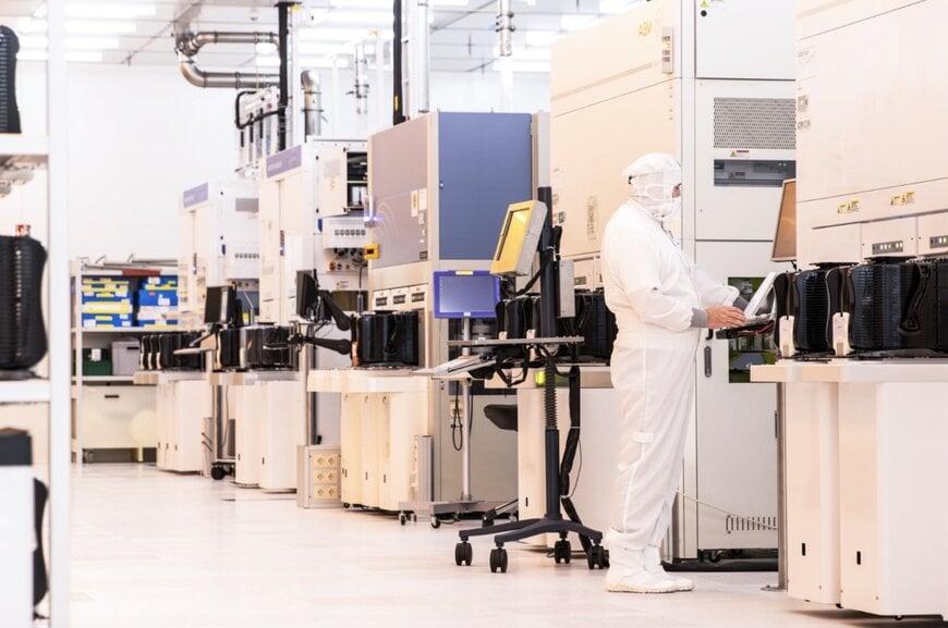
300 mm cleanroom facilities at Fraunhofer IPMS © Fraunhofer IPMS
Semiconductor architects face mounting physical and economic hurdles as traditional monolithic die scaling encounters fundamental lithographic limits and soaring fabrication costs at advanced nodes. Disaggregating systems-on-chip into modular, heterogeneous chiplets offers an alternative pathway, yet interconnecting disparate logic, memory, and analog dies introduces severe packaging challenges. Conventional wire-bonding and standard printed circuit board traces introduce high parasitic capacitance and latency bottlenecks, while monolithic integration across distinct process nodes remains cost-prohibitive. Concurrently, artificial intelligence workloads and edge inference engines face severe memory-wall limitations, demanding embedded non-volatile memory that operates with nanosecond switching speeds without excessive leakage current. Addressing these interconnected scaling constraints requires standardized pilot-line access to advanced packaging architectures—including 2.5D silicon interposers and wafer-level embedding—alongside CMOS-compatible photonics and low-voltage ferroelectric memory devices.
Heterogeneous Packaging and Quasi-Monolithic Chiplet Embedding
To support Europe’s industrial chiplet roadmap, the Fraunhofer Institute for Photonic Microsystems (IPMS) will present its packaging and device research at SEMICON Europa 2026 in Munich, highlighting contributions to the European pilot lines APECS (Advanced Packaging and Heterogeneous Integration for Electronic Components and Systems) and FAMES under the EU Chips Act's Chips for Europe Initiative. Fraunhofer IPMS contributes wafer processing, integration protocols, and system prototyping across 200 mm and 300 mm wafer platforms.
The institute's advanced packaging demonstrations focus on two complementary integration pathways:
Semiconductor architects face mounting physical and economic hurdles as traditional monolithic die scaling encounters fundamental lithographic limits and soaring fabrication costs at advanced nodes. Disaggregating systems-on-chip into modular, heterogeneous chiplets offers an alternative pathway, yet interconnecting disparate logic, memory, and analog dies introduces severe packaging challenges. Conventional wire-bonding and standard printed circuit board traces introduce high parasitic capacitance and latency bottlenecks, while monolithic integration across distinct process nodes remains cost-prohibitive. Concurrently, artificial intelligence workloads and edge inference engines face severe memory-wall limitations, demanding embedded non-volatile memory that operates with nanosecond switching speeds without excessive leakage current. Addressing these interconnected scaling constraints requires standardized pilot-line access to advanced packaging architectures—including 2.5D silicon interposers and wafer-level embedding—alongside CMOS-compatible photonics and low-voltage ferroelectric memory devices.
Heterogeneous Packaging and Quasi-Monolithic Chiplet Embedding
To support Europe’s industrial chiplet roadmap, the Fraunhofer Institute for Photonic Microsystems (IPMS) will present its packaging and device research at SEMICON Europa 2026 in Munich, highlighting contributions to the European pilot lines APECS (Advanced Packaging and Heterogeneous Integration for Electronic Components and Systems) and FAMES under the EU Chips Act's Chips for Europe Initiative. Fraunhofer IPMS contributes wafer processing, integration protocols, and system prototyping across 200 mm and 300 mm wafer platforms.
The institute's advanced packaging demonstrations focus on two complementary integration pathways:
- 2.5D Interposer Integration: Multiple chiplets—such as compute logic, high-bandwidth sensors, and specialized memory—are arranged side by side on a high-density silicon interposer layer mounted above the base package substrate. This architecture establishes short, high-density electrical interconnects that deliver data exchange rates comparable to monolithic dies while allowing each functional block to be fabricated on its optimal process node.
- Quasi-Monolithic Integration (QMI): Pursuing ultra-high-density packaging, Fraunhofer IPMS embeds bare chiplets directly into pre-structured micro-cavities (pockets) within a host silicon wafer. Following placement, the wafer surface is planarized to allow standard wafer-level thin-film redistribution layers (RDL) to interconnect the embedded dies. Fraunhofer IPMS confirmed the successful wafer-level integration of functional chiplets using this approach, achieving the initial milestone on its QMI technology roadmap.
Prof. Wenke Weinreich, Director of Fraunhofer IPMS, emphasized that next-generation electronics will depend on the tight coupling of specialized components, noting that migrating back-end packaging techniques into front-end wafer fabrication enables high-performance, energy-efficient microelectronic systems.
Low-Loss Waveguide Photonics and Hafnium-Oxide FeRAM
Beyond multi-die packaging, Fraunhofer IPMS is demonstrating wafer-scale optical interconnect and embedded memory platforms:
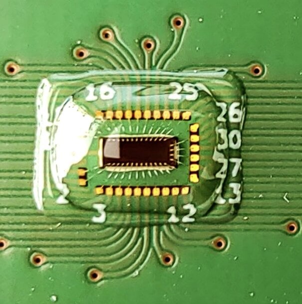
8kbit FeMFET Memory Demonstrator as chip-on board solution developed by Fraunhofer IPMS © Fraunhofer IPMS
Low-Loss Waveguide Photonics and Hafnium-Oxide FeRAM
Beyond multi-die packaging, Fraunhofer IPMS is demonstrating wafer-scale optical interconnect and embedded memory platforms:
- Silicon Nitride Photonic Platform: Available on both 200 mm and 300 mm wafer lines, the CMOS-compatible silicon nitride (SiN) waveguide platform delivers ultra-low optical propagation losses across a broad spectral band spanning the visible spectrum to the mid-infrared region. The platform provides a scalable foundation for photonic integrated circuits (PICs), optical biosensors, quantum computing interfaces, and hybrid optical-electronic transceivers.
- Hafnium Oxide Ferroelectric Memories: Leveraging ferroelectric layer stacks based on hafnium oxide, the institute offers non-volatile ferroelectric RAM (FRAM) and ferroelectric field-effect transistor (FeFET) technologies. The devices operate at sub-one-volt supply rails and achieve switching latencies in the nanosecond range. The proprietary material stacks retain ferroelectric polarization and endurance under high-temperature operating conditions, making them suitable for embedded automotive microcontrollers, on-sensor intelligence, and edge AI accelerator circuits.
External industrial partners and fabless design houses can access these technology platforms via process design kits (PDKs) and pilot-line fabrication runs, supported by Fraunhofer IPMS from initial electrical modeling through cleanroom prototyping and device characterization.
Additional Context
This section details technical specifications and competitive benchmarking not included in the original product announcement.
In advanced packaging governed by IEEE EPS (Electronics Packaging Society) and SEMI standards, 2.5D interposer integration relies on high-density Through-Silicon Vias (TSVs) and sub-micron fine-pitch copper redistribution layers to achieve interconnect wire densities exceeding several hundred lines per millimeter. By comparison, Quasi-Monolithic Integration (QMI) eliminates the interposer substrate thickness entirely by recessing chiplets into the silicon carrier wafer itself. This minimizes parasitic z-axis thermal resistance and mechanical warpage, allowing ultra-fine pitch interconnects to be patterned across die-to-wafer boundaries using standard back-end-of-line (BEOL) stepper lithography and chemical mechanical planarization (CMP). In photonic integration, transitioning from standard silicon-on-insulator (SOI) channels to stoichiometric silicon nitride waveguides expands the optical transparency window below 1.1 microns, allowing optical routing down to 405 nanometers while eliminating two-photon absorption at telecommunication wavelengths (1310 and 1550 nanometers) to handle high-power optical inputs.
Within the European and international semiconductor research and advanced packaging landscape, Fraunhofer IPMS and the APECS consortium benchmark alongside major microelectronics R&D hubs such as imec in Belgium (3D System Integration program), CEA-Leti in France, and Taiwan's ITRI. While foundry-specific commercial packaging flows—such as TSMC’s CoWoS (Chip-on-Wafer-on-Substrate) or Intel’s EMIB (Embedded Multi-die Interconnect Bridge)—are closely coupled to proprietary high-volume production lines, the APECS open pilot line provides an open-access industrial platform where European SMEs, automotive Tier-1s, and fabless startups can qualify multi-die assemblies on standard 200 mm and 300 mm tools. Furthermore, while legacy ferroelectric memories based on lead zirconate titanate (PZT) suffered from lead contamination risks in standard CMOS lines and poor scalability below 130 nanometers, utilizing doped hafnium oxide enables Fraunhofer IPMS to deposit sub-10-nanometer ferroelectric films via Atomic Layer Deposition (ALD) directly into existing CMOS BEOL metallization stacks, facilitating monolithic integration with sub-28-nanometer logic.
Edited by Romila DSilva, Induportals Editor, with AI assistance.
Additional Context
This section details technical specifications and competitive benchmarking not included in the original product announcement.
In advanced packaging governed by IEEE EPS (Electronics Packaging Society) and SEMI standards, 2.5D interposer integration relies on high-density Through-Silicon Vias (TSVs) and sub-micron fine-pitch copper redistribution layers to achieve interconnect wire densities exceeding several hundred lines per millimeter. By comparison, Quasi-Monolithic Integration (QMI) eliminates the interposer substrate thickness entirely by recessing chiplets into the silicon carrier wafer itself. This minimizes parasitic z-axis thermal resistance and mechanical warpage, allowing ultra-fine pitch interconnects to be patterned across die-to-wafer boundaries using standard back-end-of-line (BEOL) stepper lithography and chemical mechanical planarization (CMP). In photonic integration, transitioning from standard silicon-on-insulator (SOI) channels to stoichiometric silicon nitride waveguides expands the optical transparency window below 1.1 microns, allowing optical routing down to 405 nanometers while eliminating two-photon absorption at telecommunication wavelengths (1310 and 1550 nanometers) to handle high-power optical inputs.
Within the European and international semiconductor research and advanced packaging landscape, Fraunhofer IPMS and the APECS consortium benchmark alongside major microelectronics R&D hubs such as imec in Belgium (3D System Integration program), CEA-Leti in France, and Taiwan's ITRI. While foundry-specific commercial packaging flows—such as TSMC’s CoWoS (Chip-on-Wafer-on-Substrate) or Intel’s EMIB (Embedded Multi-die Interconnect Bridge)—are closely coupled to proprietary high-volume production lines, the APECS open pilot line provides an open-access industrial platform where European SMEs, automotive Tier-1s, and fabless startups can qualify multi-die assemblies on standard 200 mm and 300 mm tools. Furthermore, while legacy ferroelectric memories based on lead zirconate titanate (PZT) suffered from lead contamination risks in standard CMOS lines and poor scalability below 130 nanometers, utilizing doped hafnium oxide enables Fraunhofer IPMS to deposit sub-10-nanometer ferroelectric films via Atomic Layer Deposition (ALD) directly into existing CMOS BEOL metallization stacks, facilitating monolithic integration with sub-28-nanometer logic.
Edited by Romila DSilva, Induportals Editor, with AI assistance.
