
electronics-journal.com
23
'26
Written on Modified on
Power System-in-Package GaN Half-Bridge Integration
STMicroelectronics MasterGaN7 integrates 650V half-bridge transistors and stabilized drivers to boost efficiency, frequency, and power density across compact industrial and consumer converters.
www.st.com
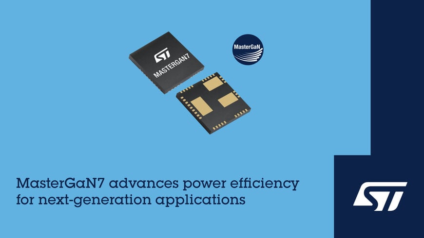
High-density power conversion in switched-mode power supplies faces thermal and board space constraints when legacy silicon MOSFETs operate at elevated switching frequencies. Wide-bandgap semiconductor devices address these limits, and the introduction of MasterGaN7 by STMicroelectronics combines two 650V enhancement-mode gallium nitride (GaN) power transistors with a dedicated high-voltage, high-frequency gate driver to resolve parasitic inductance and driver layout challenges in power adapters, industrial lighting, and renewable energy equipment.
Engineering Architecture and Operating Principles
Operating at high switching speeds exposes discrete GaN transistors to board-level parasitic inductances, which cause voltage overshoots and erratic switching behavior. MasterGaN7 eliminates long gate traces by embedding the high-side and low-side 650V GaN transistors alongside their driving circuitry in a unified 9mm x 9mm QFN package.
The system-in-package includes integrated low drop-out (LDO) regulators that supply a stabilized gate-drive potential directly to both the high-side and low-side drivers. Stabilizing gate voltage internally prevents overvoltage stress on the gate dielectric while avoiding the under-driving states that increase conduction losses. An integrated bootstrap diode powers the high-side floating driver section, further reducing external component count.
The device features an overall driver propagation delay of 45ns and supports switching frequencies up to 2MHz. To facilitate strict energy-efficiency mandates during idle periods, a dedicated pin-driven shutdown mode reduces no-load power consumption with rapid wake-up capability. Built-in interlocking logic prevents simultaneous conduction of the high-side and low-side switches, while integrated undervoltage lock-out (UVLO) and thermal shutdown safeguard the package against line drops and over-temperature events.
Technical Specifications
The power stage comprises two 650V enhancement-mode GaN high-electron-mobility transistors arranged in a half-bridge topology, supporting a maximum continuous drain current of 6A. Driven by integrated high-voltage circuitry, the package operates across switching frequencies reaching 2MHz with a matched propagation delay of 45ns, accepting standard 3.3V to 15V logic control signals with built-in input hysteresis. Hardware-level reliability is reinforced through integrated undervoltage lock-out, over-temperature thermal shutdown, and anti-cross-conduction interlocking circuitry. Housed in a standard 9mm x 9mm QFN surface-mount footprint, the device maintains operational stability across an industrial junction temperature range of -40°C to 125°C, with volume production pricing starting at $3.83 for 1,000-piece orders.
Industrial Implementation and Topologies
Operating power stages at frequencies up to 2MHz allows designers to scale down the physical footprint of reactive passive components, including planar transformers, resonant inductors, and filter capacitors. MasterGaN7 integrates into multiple primary conversion architectures, such as active clamp flyback, asymmetrical half-bridge, resonant LLC converters, synchronous inverse buck stages, power factor correction pre-regulators, and DC-to-AC inverters.
Typical deployment environments include USB Type-C Power Delivery adapters, compact chargers, industrial ballasts, stage lighting equipment, and photovoltaic microinverters. The shared footprint and pinout across the MasterGaN family allow engineering teams to scale current ratings across common circuit board layouts without redesigning core hardware. Development and prototype testing are supported via the EVLMG7 demonstration board.
Additional Context:
This section details technical specifications and competitive benchmarking not included in the original product announcement.
The transition from discrete silicon superjunction MOSFETs to monolithic and co-packaged GaN stages is driven by global efficiency regulations, including EU Ecodesign and the European Union universal USB-C charging standards (Directive 2022/2380). Discrete GaN implementations frequently suffer from package parasitic inductances that induce switch ringing and electromagnetic interference at frequencies above 500kHz. Integrated half-bridge systems-in-package resolve this layout challenge by keeping gate loop areas under several millimeters.
Within the 650V half-bridge class, MasterGaN7 competes with integrated platforms such as Navitas Semiconductor GaNFast half-bridge ICs and Power Integrations HiperLCS solutions. Navitas GaNFast ICs integrate autonomous drive and loss-less current sensing into single power stages, whereas the MasterGaN7 architecture retains independent high-side and low-side digital control inputs. This preserves full flexibility for third-party microcontrollers and external analog controllers executing peak current-mode control or zero-voltage switching algorithms without requiring proprietary PWM controllers. Furthermore, while standalone discrete GaN HEMTs require external linear regulators or specialized multi-rail gate-drive ICs to prevent gate breakdown, MasterGaN7 embeds dedicated internal LDOs that accept standard system supply rails directly.
Edited by Sucithra Mani, Induportals editor – adapted by AI.
www.st.com
