
electronics-journal.com
24
'26
Written on Modified on
Accelerating System Design on Advanced Semiconductor Nodes
Synopsys and TSMC collaborate to deploy automated EDA workflows and unified multiphysics verification for high-performance computing components.
www.synopsys.com
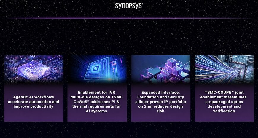
Synopsys and TSMC are expanding their technical collaboration to integrate agentic AI-assisted engineering workflows within Electronic Design Automation (EDA) platforms. The cooperation focuses on streamlining the design, verification, and packaging of complex multi-die systems and high-performance computing (HPC) hardware for advanced semiconductor applications.
Managing Scale in Heterogeneous Integration
The development of modern hardware requires integrating distinct logic, memory, and optical chiplets into a single package. Designing these heterogeneous multi-die architectures introduces severe power integrity, thermal management, and spatial floorplanning challenges that exceed traditional manual engineering capabilities. Synopsys and TSMC established this collaboration to couple Synopsys's computational EDA software directly with TSMC's proprietary silicon process nodes and 3DFabric packaging methodologies.
This deep integration allows hardware engineers to validate physical layout, power delivery, and thermal tolerances accurately before committing to physical silicon production. Michael Buehler-Garcia, Senior Vice President at Synopsys, noted that the joint innovations address the required continuum of silicon-to-systems co-design capabilities necessary for the development of high-performance computing systems.
Certified EDA Workflows and AI Automation
A primary output of the collaboration is the certification of Synopsys EDA flows for the TSMC A14 process technology. This certification provides hardware developers with a validated digital and analog implementation framework, ensuring that design convergence meets the strict physical parameters of the A14 node. In analog design specifically, the partnership achieved device routing enablement on A14, a mechanism that automates complex place-and-route tasks to increase layout productivity.
To address the complexity of heterogeneous packaging, the partners implemented agentic AI capabilities within the Synopsys 3DIC Compiler platform. This specific workflow utilizes AI to automate chiplet floorplanning co-optimization, accelerating the spatial arrangement of multiple dies while adhering to the physical constraints of TSMC 3DFabric technologies. Furthermore, for integrated voltage regulators (IVRs), which are critical for stabilizing power delivery in multi-die arrays, the 3DIC platform now permits engineers to co-design and simulate IVR structures directly on TSMC CoWoS (Chip-on-Wafer-on-Substrate) packaging.
Optical Interconnects and Physical IP
As data bandwidth requirements escalate, the cooperation also targets co-packaged optics (CPO). Synopsys and TSMC have developed an integrated photonic and electronic co-design flow for TSMC COUPE technology. This workflow unifies 3DIC physical implementation with multiphysics analysis, allowing engineers to verify advanced optical interconnect architectures without utilizing disjointed software toolchains.
At the hardware level, Synopsys continues to expand its portfolio of silicon-proven physical intellectual property (IP) optimized for TSMC's 3nm and 2nm nodes. The collaboration recently achieved physical tape-out milestones on the TSMC N2P process for critical connectivity and memory interfaces, including PCIe 7.0, HBM4, and 224G Ethernet PHY. For multi-die connectivity, Synopsys validated its UCIe-A 32G/40G IP on a TSMC N3P test chip utilizing a CoWoS-S interposer, confirming the stability of high-speed die-to-die communication necessary for scaled HPC workloads.
Edited by Aishwarya Mambet, Induportals Editor, with AI assistance.
www.synopsys.com
