
electronics-journal.com
10
'26
Written on Modified on
Microchip Launches 1.2 V Clock Buffers for Advanced SoCs & FPGAs
SY757xx buffers provide voltage translation, ultra-low jitter and broad frequency support, simplifying clock distribution while reducing components and preserving signal integrity.
www.microchip.com
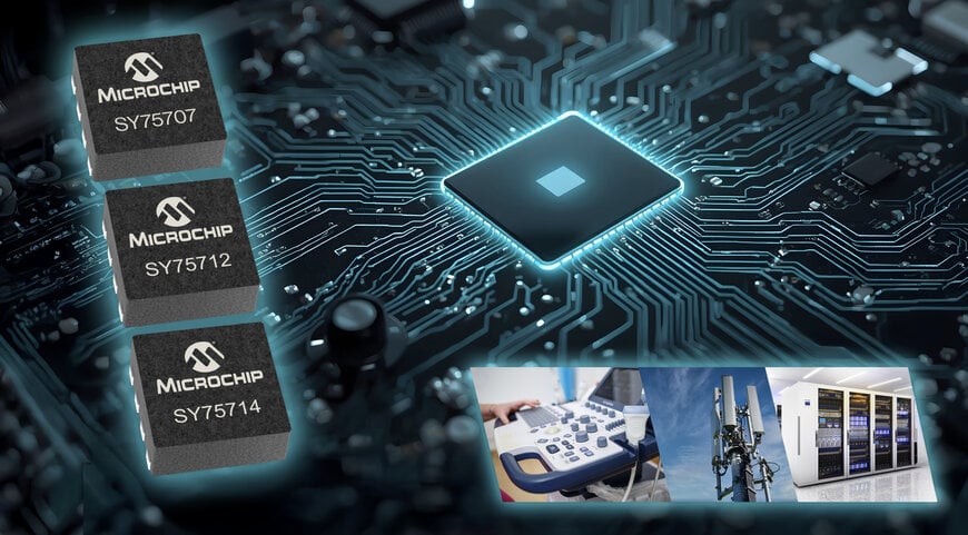
Microchip Technology has introduced the SY757xx line of integrated circuit clock buffers, designed to route timing signals between legacy supply rails and core logic operating at 1.2V. The components target digital supply chain infrastructure, high-performance computing, artificial intelligence accelerators, industrial automation, and high-density networking architectures.
Interfacing Advanced FinFET Architectures and Legacy Rails
Silicon architectures fabricated on sub-nanometer FinFET nodes operate at reduced core voltages, creating an input threshold mismatch with standard system rails. Connecting legacy 3.3V, 2.5V, or 1.8V oscillators directly to modern processors requires intermediary level translation. System designers historically addressed this interface using discrete resistor-divider networks or dual-supply level shifters. Passive divider networks introduce capacitive loading, reduce transition slew rates, degrade duty-cycle symmetry, and increase board bill-of-materials.
The SY757xx devices replace discrete networks by providing active level conversion on a single die. The architecture accepts single-ended or differential input signals ranging from 1.2V to 3.3V and translates them down to 1.2V to 1.8V LVCMOS signal outputs. The operating frequency range extends from direct current (0 Hz) up to 250 MHz, protecting clock duty-cycle fidelity and eliminating the signal degradation associated with passive attenuators.
Signal Integrity Parameters and Additive Jitter Performance
High-speed digital processing platforms require minimal phase noise to maintain timing margins across parallel buses and serial links. The SY757xx family specifies additive phase jitter as low as 26 femtoseconds (fs), preventing significant noise contribution to the original clock source.
Maintaining low jitter across wide operating ranges enables deployment in embedded vision systems, machine learning edge inference accelerators, and communication infrastructure where clock edge uncertainty degrades bit-error rates. Integrated active buffering also resolves impedance matching issues, stabilizing signal integrity between oscillators, FPGAs, system-on-chip devices, and central processing units.
Device Variants, Packaging Options, and Commercial Production
The initial deployment of the product family includes three devices released for high-volume manufacturing: the SY75707TWL-TR, the SY75712TWL-TR, and the SY75714TWL-TR. Unit pricing ranges from $0.50 to $0.83 in production orders of 10,000 pieces.
The SY75707TWL-TR converts differential input signals to two LVCMOS outputs and is packaged in an 8-pin Very-thin Dual Flat No-lead (VDFN) footprint. The SY75712TWL-TR and SY75714TWL-TR provide two and four LVCMOS outputs respectively, with rail operations between 1.2V and 1.8V, housed in 8-pin Thin Dual Flat No-lead (TDFN) packages.
Eight additional family variants are currently sampling in 8-pin VDFN packages to address distinct fanout configurations. These configurations cover single-ended 1.2V to 3.3V inputs, single-ended 1.2V to 1.8V inputs, differential 1.8V to 3.3V inputs, and integrated output-enable control features.
Additional Context:
This section details technical specifications and competitive benchmarking not included in the original product announcement
Clock distribution devices serving lower I/O voltages compete directly against timing portfolios from suppliers such as Texas Instruments, Skyworks Solutions, and Renesas Electronics. Standard LVCMOS buffers in the market historically supported outputs down to 1.5V or 1.8V, often requiring dual-rail architectures (VDDO separate from VDDI) with separate external decoupling capacitors to translate down to 1.2V logic thresholds.
In high-speed timing distribution, Texas Instruments offers devices such as the LMK00101 and the CDCLVC11xx family, which deliver low phase noise and single-ended distribution. However, many universal buffers in this operational tier require external supply rail splits or exhibit additive jitter metrics ranging from 50 fs to several hundred femtoseconds when operating near lower supply boundaries. Similarly, Renesas portfolio buffers covering differential-to-LVCMOS translation traditionally focus on PCIe and telecom standards with output swings standardizing at 1.8V, 2.5V, or 3.3V.
By establishing an additive jitter baseline of 26 fs at a native 1.2V output rail in an 8-pin VDFN footprint, the SY757xx addresses a specific hardware boundary condition: driving low-voltage FinFET clock trees directly from multi-voltage system rails without exceeding strict jitter budgets or requiring dedicated secondary power planes.
Edited by Natania Lyngdoh, Induportals editor, assisted by AI.
www.microchip.com
