
electronics-journal.com
13
'26
Written on Modified on
KIOXIA and Sandisk Launch 10G QLC NAND
The 332-layer 3D flash memory achieves 37 Gb/mm² to power AI and cloud infrastructures.
europe.kioxia.com
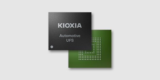
KIOXIA Europe GmbH has announced that KIOXIA Corporation and Sandisk Corporation have unveiled their 10th-generation Quad-Level Cell (QLC) 3D flash memory technology. Thanks to a 332-layer architecture and an optimized cell array design, this innovation offers a bit density increase of up to 60% compared to 8th-generation technology. With a density exceeding 37 Gb/mm², it sets a new industry record in storage for capacity, performance, and power efficiency.
Architectural Innovations and Record Bandwidth
Leveraging CBA (CMOS Directly Bonded to Array) technology—which bonds the CMOS logic and memory array manufactured on separate wafers with high-precision alignment—this new generation is the industry's first QLC 3D flash memory to achieve a 4.8 Gb/s interface, enabled by the Toggle DDR6.0 standard and the Separate Command Address (SCA) protocol. Furthermore, Power-Isolated Low-Tapped Termination (PI-LTT) technology optimizes the power efficiency of I/O data transfers. According to Axel Störmann (Vice President and CTO of KIOXIA Europe GmbH) and Alper Ilkbahar (CTO of Sandisk), these advancements in density and bandwidth are essential to meet the unprecedented growth in workloads related to hyperscale data centers, generative AI, and agentic and physical systems.
Additional Context: Technological Background and Market Dynamics
This section provides technological and market context not explicitly detailed in the original release.
The continuous increase in the number of layers in 3D NAND memory is the industry's preferred method for massively scaling storage capacity without expanding the chip's physical footprint. QLC technology enables the storage of four bits of data per cell, offering an ultra-competitive cost per gigabyte. The CBA architecture represents a major breakthrough in manufacturing: by producing the logic circuit and the memory cells on two separate silicon wafers before bonding them, manufacturers can utilize the most suitable etching processes for each part of the chip. This breaks thermal bottlenecks and achieves the extreme read/write speeds essential for the continuous operation of Large Language Models (LLMs) in modern server farms.
Edited by Lekshman Ramdas, Induportals editor – adapted by AI.
www.kioxia.com
