
electronics-journal.com
18
'26
Written on Modified on
Integration of System-Level Simulation in Photonic Design Automation
Keysight Technologies integrates newly acquired VPIphotonics software suites to enable unified electrical-optical-electrical link validation for high-performance data center infrastructure.
www.keysight.com
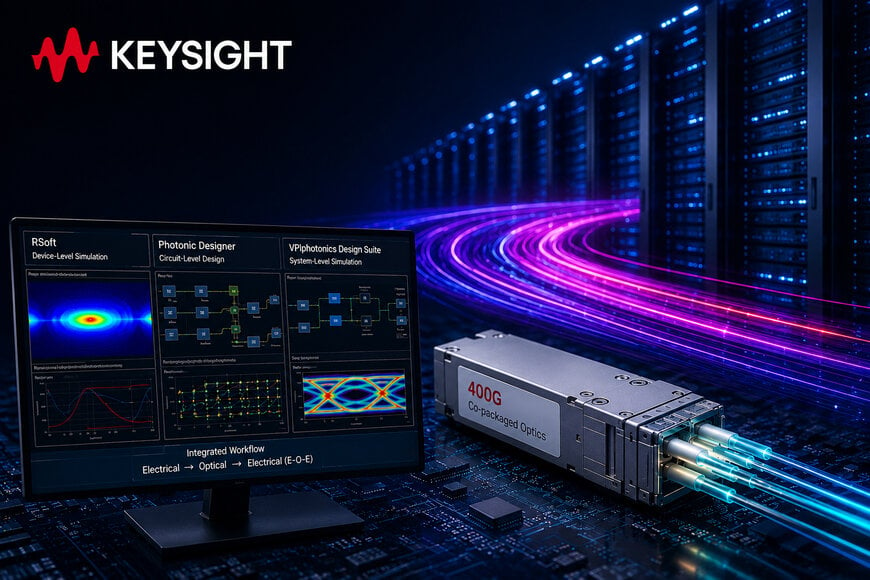
Keysight Technologies has expanded its digital infrastructure portfolio by incorporating system-level simulation software to establish a continuous, multi-domain photonic design automation workflow. The integrated platform addresses the increasing complexity of silicon photonics and co-packaged optics architectures deployed within high-speed computing networks.
Operational Constraints in Advanced Optical Communications
The escalation of data center capacities and artificial intelligence workloads requires optical interconnects capable of operating at transmission speeds exceeding 1 THz. Designing these high-bandwidth infrastructure components requires managing interactions between device physics, circuit layouts, and full system behavior. Traditionally, engineering teams relied on separate electrical and optical design environments, necessitating manual data handoffs that increased development timelines and introduced simulation errors. Resolving these validation bottlenecks required combining hardware-level electronic design automation software with specialized photonic transmission simulation platforms.
Functional Architecture and Software Integration
The expanded design portfolio establishes a hierarchical workflow spanning from structural components to end-to-end link simulation. Initial structural simulation relies on RSoft software to model discrete device-level physics, including optical waveguides, diffraction gratings, electro-optic modulators, and semiconductor laser sources. Circuit-level verification is executed via Photonic Designer to simulate integrated photonic circuits.
The integration of the VPIphotonics Design Suite introduces system-level simulation to this sequence. A core functional mechanism of this framework is the VPI Optical Link interface within Keysight Advanced Design System (ADS). This architecture allows engineers to perform end-to-end electrical-optical-electrical (E-O-E) transceiver path analysis within a singular processing environment. The software models signal degradation across the complete channel, allowing the prediction of operational performance parameters, such as the overall bit error rate (BER).
Infrastructure Alignment and Application Framework
The primary application areas for this integrated design workflow encompass silicon photonics development, co-packaged optics engineering, and high-density semiconductor manufacturing for digital infrastructure. The simulation environment directly interfaces with high-speed digital tools and laboratory test instruments. This technical link allows developers to align mathematical simulation models with physical bench measurements, establishing a closed-loop validation process.
By identifying signal integrity issues and behavioral deviations prior to physical fabrication, engineering teams reduce the number of physical prototyping iterations required for system validation. This programmatic alignment accelerates deployment timelines for communication sub-systems while ensuring adherence to rigid bit error rate tolerances in high-frequency network environments.
Edited by Sucithra Mani, Induportals editor – adapted by AI.
www.keysight.com
