
electronics-journal.com
08
'26
Written on Modified on
Capacitive sensors for wafer planarization control
Micro-Epsilon provides capacitive distance sensors for real-time planarization measurement in hybrid bonding processes for semiconductor manufacturing.
www.micro-epsilon.com
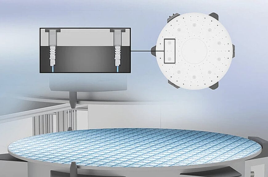
Capacitive distance sensors are being used in semiconductor manufacturing to measure wafer planarization in real time during hybrid bonding processes. The technology supports adaptive alignment of bonding units by detecting shape deviations and height differences across wafer surfaces.
Real-time planarization measurement in hybrid bonding
Hybrid bonding is an advanced semiconductor interconnection technology in which wafers or semiconductor dies are directly connected through copper contact surfaces without the use of conventional solder bumps. The process is increasingly used in die-to-wafer (D2W) and wafer-to-wafer (W2W) manufacturing architectures for high-density semiconductor packaging.
In these applications, wafer planarization is a critical parameter affecting bonding stability, electrical connectivity, and yield rates. Even minor surface deviations can lead to alignment errors or incomplete bonding during the joining process.
Capacitive distance sensors enable non-contact measurement of wafer surface geometry, including bending, twisting, and localized warpage. The sensors provide high-resolution measurement data required for adaptive positioning and leveling of bonding equipment within the semiconductor production environment.
Inline wafer inspection and adaptive leveling
Depending on the measurement task, sensor arrays scan the surfaces of the upper and lower wafers to detect local elevations, depressions, inclinations, or overall wafer bow. The resulting measurement data is integrated into active position correction systems for wafer stages.
If height deviations are detected, the bonding unit can be adjusted in the Z-axis using piezo actuators or precision positioning systems. For very small semiconductor dies, segmented chuck surfaces can also be leveled locally to improve positioning accuracy.
This inline planarization control supports stable hybrid bonding processes and contributes to improved process repeatability in advanced semiconductor packaging.
Non-contact measurement for semiconductor process stability
Capacitive measurement technology is particularly suited to semiconductor manufacturing because it enables non-contact operation with high resolution and minimal influence on sensitive wafer surfaces. The sensors support continuous monitoring of form deviations without introducing mechanical stress or contamination risks. The compact sensor design and vacuum-compatible construction enable integration into semiconductor production environments, including process chambers and automated wafer handling systems.
Applications in advanced semiconductor packaging
The technology is suitable for advanced packaging applications requiring precise wafer alignment and high process stability. Typical application areas include 3D semiconductor integration, heterogeneous integration, high-bandwidth memory packaging, and chiplet-based architectures.
As semiconductor manufacturers continue increasing interconnect density and reducing package dimensions, precise planarization measurement becomes increasingly important for maintaining bonding quality and production yields across high-volume manufacturing environments.
Additional Context: technical specifications and competitive benchmarking not included in the original announcement
In semiconductor metrology and wafer inspection, manufacturers such as KLA, Keyence, and Lion Precision offer comparable non-contact measurement technologies for wafer positioning and planarization control. Capacitive sensing systems are commonly benchmarked based on measurement resolution, bandwidth, thermal stability, vacuum compatibility, and response time.
In hybrid bonding applications, planarization tolerances are often measured in the sub-micrometer range, requiring high-speed sensors capable of detecting minimal surface deviations during inline processing. Competing technologies may also include optical interferometry and confocal chromatic measurement systems, although capacitive sensors are often preferred for conductive surfaces due to their high sensitivity and compact integration capability.
The presented solution is differentiated primarily through the combination of vacuum-compatible sensor construction, inline real-time planarization monitoring, adaptive leveling support, and integration into active wafer-stage positioning systems for D2W and W2W hybrid bonding applications.
Edited by Maria Brueva, Induportals editor – adapted by AI.
www.micro-epsilon.com
