
RISC-V and Photonics Integration for AI Chiplets
CEA-Leti, CEA-List and Powerchip Semiconductor Manufacturing Corporation (PSMC) collaborate to combine RISC-V computing and silicon photonics within 3D semiconductor integration platforms for AI systems.
www.cea.fr
CEA-Leti and CEA-List, institutes of the French Alternative Energies and Atomic Energy Commission, are working with Powerchip Semiconductor Manufacturing Corporation to integrate RISC-V processor architectures and silicon photonics into 3D semiconductor integration platforms. The cooperation targets artificial intelligence systems requiring high-bandwidth data transfer and improved energy efficiency.
Context of the Cooperation
CEA-Leti contributes expertise in micro- and nanotechnology, particularly silicon photonics, while CEA-List develops advanced digital architectures, including RISC-V-based processor designs. PSMC provides manufacturing capabilities based on 3D stacking and interposer technologies.
The collaboration addresses constraints in conventional semiconductor scaling. Electrical interconnects based on copper face increasing limitations in bandwidth and power consumption, particularly in AI workloads where large data volumes must be transferred between compute elements. At the same time, fixed processor architectures limit optimization for specific applications. The cooperation combines complementary capabilities to address both data movement and compute flexibility at system level.
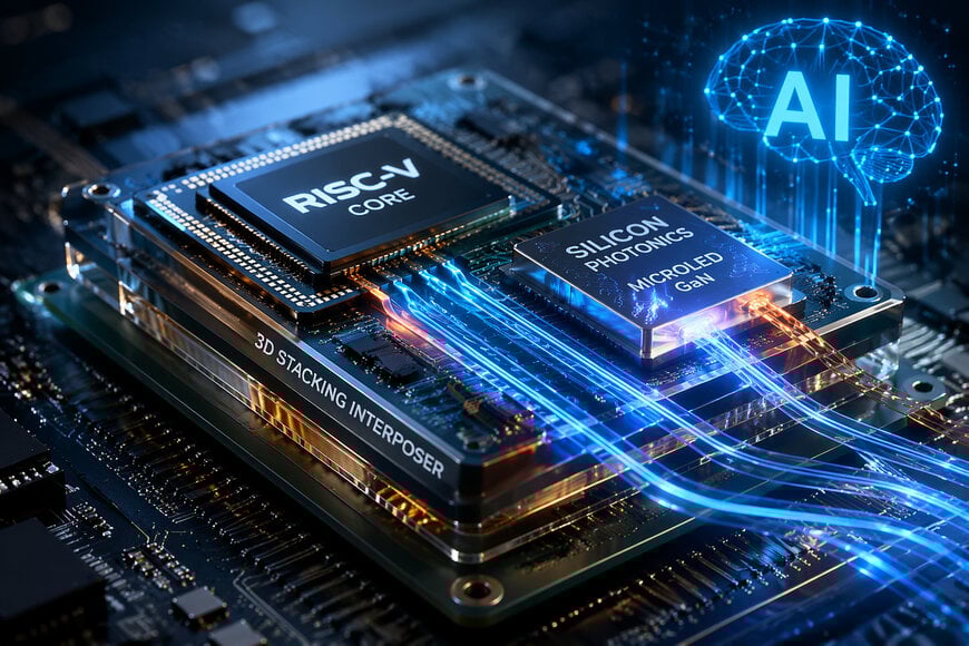
Technical Solution and Responsibilities
The technical approach combines customizable RISC-V processor cores with silicon photonics interconnects integrated into a chiplet-based architecture. CEA-List develops the processor IP, enabling adaptation of instruction sets and system configurations to application-specific requirements. CEA-Leti provides optical interconnect technologies based on silicon photonics, including short-reach communication links designed to increase bandwidth while reducing energy per transmitted bit.
PSMC integrates these components within its 3D stacking and interposer platforms. The interposer enables high-density interconnection between chiplets, while photonic links replace part of the electrical communication pathways. MicroLED-based GaN light sources are used to drive optical transmission, supporting higher data rates within constrained power budgets.
Deployment and Integration
The solution is designed for integration into PSMC’s existing foundry processes. Implementation follows a co-design approach, where compute, interconnect, and packaging layers are developed in parallel to ensure compatibility in terms of signal integrity, thermal behavior, and manufacturing constraints.
Initial phases focus on validating photonic interconnect performance and RISC-V-based compute blocks, followed by system-level integration within 3D stacked devices. The use of established interposer technology allows integration with existing semiconductor workflows, reducing barriers to industrial deployment.
Applications and Use Cases
The architecture targets AI accelerators, data center processors, and edge computing systems where high data throughput and energy-efficient processing are required. Optical interconnects reduce latency and energy consumption in data movement, while modular RISC-V architectures allow tailoring compute resources to specific workloads.
Expected Impact
The integration of photonic communication within 3D chiplet architectures enables higher bandwidth density compared to conventional electrical interconnects. Combined with configurable RISC-V processing, this approach supports scalable system design aligned with the requirements of modern digital infrastructure.
The cooperation illustrates how combining semiconductor manufacturing, processor design, and photonics can address performance and energy limitations in next-generation AI systems without relying solely on transistor scaling.
Edited by an industrial journalist Sucithra Mani with AI assistance.
www.cea.com
