
electronics-journal.com
07
'26
Written on Modified on
Sub-Terahertz Semiconductor Characterization Method Simplifies On-Wafer Testing
Keysight, University of Glasgow, NPL, and MPI Corporation have demonstrated a continuous 250 GHz on-wafer measurement methodology for sub-terahertz semiconductor research.
www.keysight.com
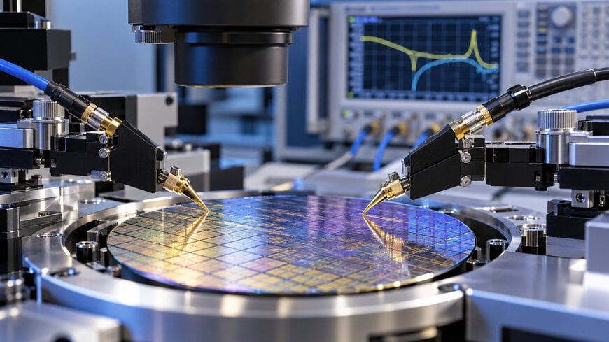
As semiconductor design pushes into millimeter-wave and sub-terahertz frequencies for advanced communications and high-frequency electronics, engineers face significant hurdles in characterizing active devices like indium phosphide high-electron-mobility transistors. Traditional characterization approaches often demand multiple instrument setups, frequent band changes, and repeated calibrations to cover wide frequency spans. This fragmented workflow introduces mechanical variations, increases setup complexity, and complicates accurate broadband device modeling. To address this industrial testing bottleneck, Keysight Technologies, the University of Glasgow, the National Physical Laboratory, and MPI Corporation have developed a unified measurement methodology capable of continuous on-wafer characterization from near DC up to 250 GHz using a single sweep.
Engineering Mechanism and Measurement Architecture
The collaborative development integrates specialized instrumentation, advanced device design, precision probing, and metrological calibration into a single cohesive ecosystem. At the core of the test setup is Keysight's PNA-X Vector Network Analyzer coupled with a Single-Sweep 250 GHz Frequency Extender and a Precision Source/Measure Unit. This hardware architecture is paired with MPI Corporation's broadband on-wafer probing technology and calibration software, alongside the University of Glasgow's indium phosphide high-electron-mobility transistor devices and custom calibration standards. National Physical Laboratory contributed high-frequency metrology and calibration methodologies to verify measurement integrity.
By combining these systems, the methodology enables continuous measurement across the entire frequency spectrum with a single probe touchdown. This eliminates the necessity for manual probe lifting, hardware reconfiguration, and multi-band connection changes. Furthermore, built-in source filtering and broadband source power calibration ensure high signal purity directly at the probe-tip, addressing the signal degradation and reflection issues common at sub-terahertz frequencies.
Industrial Applications and Operational Benefits
Accurate broadband characterization is crucial for research and development teams working on high-frequency monolithic microwave integrated circuits, next-generation wireless communications, and high-speed radar systems. Indium phosphide high-electron-mobility transistors are widely deployed in high-power, low-noise amplification circuits operating well into the terahertz domain. By streamlining the characterization workflow, the new methodology significantly reduces measurement time, minimizes human error introduced by repeated probe positioning, and yields consistent S-parameter data required for reliable active device modeling.
Thierry Locquette, Vice President of Sales for Europe, Middle East, and Africa at Keysight, noted that characterizing devices continuously from near DC to 250 GHz in a single sweep simplifies the measurement process for researchers developing next-generation semiconductor technologies. By aligning instrumentation, device engineering, probing, and metrology, the collaboration establishes a practical framework for generating reliable broadband data. Dr. Xiaobang Shang, Principal Scientist and On-wafer Measurement Lead at National Physical Laboratory, emphasized that precise on-wafer metrology remains essential for reliable device development in millimeter-wave and sub-terahertz spectrums. Matthew White, Director of Business Development at MPI Corporation, added that extending characterization to 250 GHz requires the probing, calibration, and measurement platforms to operate as an integrated system, allowing researchers to accelerate device development with greater confidence.
Additional Context:
This section details technical specifications and competitive benchmarking not included in the original product announcement.
Broadband on-wafer characterization past 110 GHz traditionally required waveguide band-switching, where engineers manually or automatically swapped frequency extender modules (such as WR-10, WR-06, and WR-03 bands) to cover D-band and H-band frequencies. Each band change historically required separate calibration routines, such as Line-Reflect-Line or Thru-Reflect-Line standards, increasing the risk of random calibration errors and mechanical wear on probe tips. Single-sweep frequency extension architectures eliminate inter-band mismatch uncertainties and reduce thermal drift associated with prolonged multi-stage testing sessions. Indium phosphide high-electron-mobility transistors remain a benchmark semiconductor technology for ultra-high cutoff frequencies, often outperforming gallium nitride and silicon germanium counterparts in raw transit frequency metrics, making high-accuracy sub-terahertz vector network analyzer characterization a critical path requirement for millimeter-wave semiconductor engineering.
Edited by Sucithra Mani, Induportals editor – adapted by AI.
www.keysight.com
