
electronics-journal.com
05
'26
Written on Modified on
Gallium Nitride RF Chip Architecture Advances High-Frequency Systems
Northrop Grumman developed the FORTITUDE microchip to resolve radio frequency spectrum congestion across defense and commercial telecommunications infrastructure.
www.northropgrumman.com
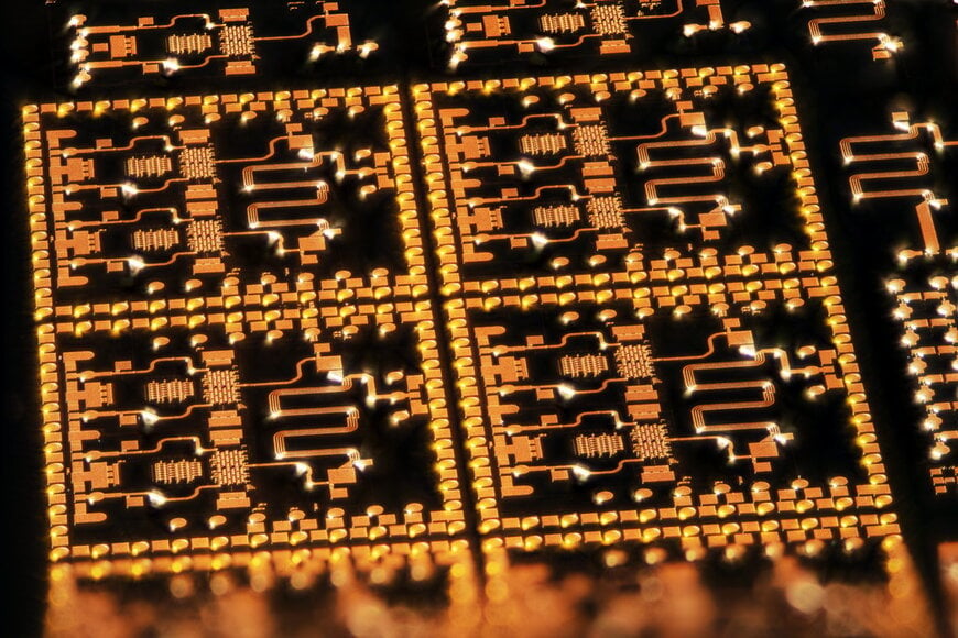
Congested electromagnetic operating environments and rising throughput requirements present persistent thermal and linearity challenges for high-frequency radio frequency communications, demanding hardware capable of operating cleanly across expansive spectrum bands. The gallium nitride semiconductor platform addresses these operational constraints by consolidating wideband signal processing into a single integrated component designed for aerospace, defense, and advanced civilian communications networks.
Electromagnetic Spectrum Processing and Signal Linearity
Modern wireless payloads and radar arrays encounter severe signal degradation when processing data across saturated frequency allocations. Conventional front-end architectures often require complex filtering networks and distributed amplifier stages to suppress intermodulation distortion, adding significant mass and thermal burden to spaceborne and airborne systems.
The hardware implementation relies on gallium nitride on silicon carbide device fabrication, previously designated as the Super Lattice Castellated Field Effect Transistor. By structuring the transistor channels into three-dimensional castellated geometries, the semiconductor architecture increases electron carrier density while improving electrostatic control across the gate region. This physical configuration enables the single-die device to process broad frequency swaths while mitigating phase noise and thermal throttling.
Performance Metrics Across Core RF Subsystems
Replacing discrete multi-stage transceiver chains with a monolithic millimeter-scale die directly alters radio frequency payload engineering. The architecture yields measurable performance improvements:
- Threefold increase in output power density compared to conventional solid-state RF devices.
- Twentyfold improvement in signal quality metrics, lowering spurious emissions and reducing error vector magnitude.
- Monolithic integration scaling down to the physical footprint of a single grain of rice.
- Component-level consolidation replacing dozens of discrete tuning, amplification, and matching parts.
Integration Across Defense and Telecommunications Workflows
The microchip functions as an active front-end amplification and signal distribution engine across several industrial and operational domains.
In orbital platforms, satellite payloads utilize the high power-to-mass ratio to reduce total launch weight while expanding usable transponder bandwidth. Electronic warfare and radar installations leverage the dynamic spectrum coverage to maintain continuous situational awareness, filtering out multi-path interference and dense electronic countermeasures.
For terrestrial navigation, military GPS receivers integrate the device to prevent hostile jamming signals from degrading positioning accuracy. In emerging civilian 6G networks and high-throughput millimeter-wave backhaul links, the high output power and reduced power consumption facilitate dense data transmission without requiring bulky active-cooling assemblies at the base station level.
Additional Context
This section details technical specifications and competitive benchmarking not included in the original product announcement.
Gallium nitride semiconductors have largely superseded traditional gallium arsenide and silicon complementary metal-oxide-semiconductor platforms in wideband high-power applications due to the material bandgap of 3.4 electron volts. Wide-bandgap semiconductors support significantly higher breakdown electric fields, which allows power amplifiers to operate at higher voltages without dielectric breakdown.
Benchmark comparisons within defense microelectronics indicate that traditional planar GaN high-electron-mobility transistors achieve typical power densities ranging from 5 to 8 watts per millimeter in the X-band and Ku-band regimes. Castellated multi-gate architectures improve upon standard high-electron-mobility transistor designs by optimizing heat dissipation and charge transport across sub-micron channel lengths. This transistor-level advancement directly aligns with Department of Defense microelectronics initiatives prioritizing domestic supply-chain resilience, lower size, weight, and power consumption, and direct-conversion transceivers capable of software-defined reconfiguration across Ka-band, V-band, and sub-terahertz frequencies.
Edited by Evgeny Churilov, Induportals Media - Adapted by AI.
www.northropgrumman.com
The microchip functions as an active front-end amplification and signal distribution engine across several industrial and operational domains.
In orbital platforms, satellite payloads utilize the high power-to-mass ratio to reduce total launch weight while expanding usable transponder bandwidth. Electronic warfare and radar installations leverage the dynamic spectrum coverage to maintain continuous situational awareness, filtering out multi-path interference and dense electronic countermeasures.
For terrestrial navigation, military GPS receivers integrate the device to prevent hostile jamming signals from degrading positioning accuracy. In emerging civilian 6G networks and high-throughput millimeter-wave backhaul links, the high output power and reduced power consumption facilitate dense data transmission without requiring bulky active-cooling assemblies at the base station level.
Additional Context
This section details technical specifications and competitive benchmarking not included in the original product announcement.
Gallium nitride semiconductors have largely superseded traditional gallium arsenide and silicon complementary metal-oxide-semiconductor platforms in wideband high-power applications due to the material bandgap of 3.4 electron volts. Wide-bandgap semiconductors support significantly higher breakdown electric fields, which allows power amplifiers to operate at higher voltages without dielectric breakdown.
Benchmark comparisons within defense microelectronics indicate that traditional planar GaN high-electron-mobility transistors achieve typical power densities ranging from 5 to 8 watts per millimeter in the X-band and Ku-band regimes. Castellated multi-gate architectures improve upon standard high-electron-mobility transistor designs by optimizing heat dissipation and charge transport across sub-micron channel lengths. This transistor-level advancement directly aligns with Department of Defense microelectronics initiatives prioritizing domestic supply-chain resilience, lower size, weight, and power consumption, and direct-conversion transceivers capable of software-defined reconfiguration across Ka-band, V-band, and sub-terahertz frequencies.
Edited by Evgeny Churilov, Induportals Media - Adapted by AI.
www.northropgrumman.com
