
electronics-journal.com
17
'26
Written on Modified on
onsemi Introduces Embedded Power Platform for Higher Power Density
Silicon wafer packaging integrates multiple dies and optimizes electrical, thermal and mechanical performance for AI infrastructure, electric vehicles and industrial applications.
www.onsemi.com
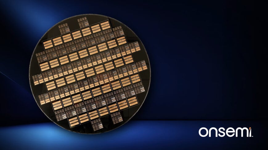
onsemi Embedded Power Platform Wafer
onsemi has introduced the Embedded Power Platform (EPP) to consolidate power electronics, mechanical support, and thermal dissipation into a unified wafer-level architecture. The manufacturing approach addresses growing electrical delivery constraints in artificial intelligence computing facilities, electric vehicle drivetrains, and industrial automation equipment.
Wafer-Level Integration and Parasitic Inductance Reduction
Conventional power electronic packaging relies on a sequential design flow where discrete power semiconductor dies are attached to ceramic substrates, wire-bonded to external terminals, and encased in plastic molding compounds. This mechanical assembly method introduces parasitic loop inductance that restricts switching frequencies and creates thermal interfaces with elevated thermal resistance.
The Embedded Power Platform converts the 300 mm (12-inch) silicon wafer into the functional package foundation. Within a cleanroom fabrication line, heterogeneous semiconductor dies—including silicon, silicon carbide (SiC), and gallium nitride (GaN)—are embedded alongside gate drivers and controller circuits. Planar wafer-level copper redistribution layers (RDLs) and vertical conductive vias replace conventional wire bonds. This configuration shortens current path lengths, minimizes loop inductance, and enables stable high-frequency switching with reduced switching losses.
Early Automotive and Data Center Deployments
In data center power distribution, rising server rack densities require power delivery systems to occupy minimal rack footprint while dissipating heat efficiently. In an initial solid-state circuit breaker application evaluated on the platform, the integrated package achieved an approximate 50% reduction in physical volume and operated 20% cooler compared to existing discrete assemblies.
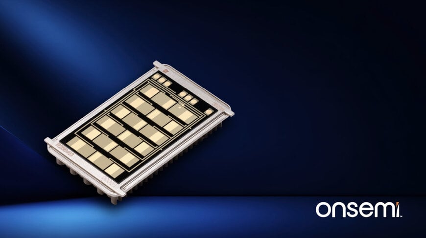
onsemi Embedded Power Platform Chip
For electrified mobility, vehicle traction inverters built on the architecture achieve up to four times higher power density and a 15% reduction in electrical power losses compared to conventional wire-bonded power modules. The unified architecture supports scalable power stages across different vehicle segments, allowing original equipment manufacturers to reuse inverter designs. Subaru Corporation has entered an early technology engagement with onsemi to evaluate the platform, utilizing simulation models and early engineering samples to assess drivetrain integration.
Additional Context:
This section details technical specifications and competitive benchmarking not included in the original product announcement
Within the high-power semiconductor packaging market, this architecture competes with discrete embedded die packaging methods and advanced power module concepts, including printed circuit board (PCB) embedding technologies developed by AT&S and Schweizer Electronic, as well as molded interconnect substrate (MIS) power modules from suppliers such as Infineon Technologies and STMicroelectronics.
A fundamental technical distinction lies in the substrate medium and interconnect fabrication methodology. Industrial embedded power solutions typically rely on organic FR-4 or bismaleimide-triazine (BT) resin laminates, in which dies are embedded into drilled cavities within multilayer PCB cores. While organic substrate embedding reduces loop inductance compared to wire bonds, it remains constrained by the thermal conductivity of organic prepregs (typically below 1 to 3 W/m·K) and PCB manufacturing design rules, which feature line widths and spaces measured in tens of micrometers.
By contrast, using a 300 mm monocrystalline silicon wafer leverages the natural thermal conductivity of bulk silicon (approximately 148 W/m·K at room temperature), functioning directly as an integrated heat-spreading layer and eliminating thick thermal interface materials. Furthermore, semiconductor-grade thin-film copper redistribution layers achieve line and space resolutions below 5 micrometers. This micro-scale lithographic routing permits tightly coupled driver-to-gate loops with sub-nanohenry loop inductances. Such low inductance is essential to suppress voltage overshoot and false turn-on events in ultra-fast wide-bandgap GaN and SiC switches during high-slew-rate transients exceeding 100 V/ns.
Edited by Natania Lyngdoh, Induportals editor, assisted by AI.
www.onsemi.com
onsemi has introduced the Embedded Power Platform (EPP) to consolidate power electronics, mechanical support, and thermal dissipation into a unified wafer-level architecture. The manufacturing approach addresses growing electrical delivery constraints in artificial intelligence computing facilities, electric vehicle drivetrains, and industrial automation equipment.
Wafer-Level Integration and Parasitic Inductance Reduction
Conventional power electronic packaging relies on a sequential design flow where discrete power semiconductor dies are attached to ceramic substrates, wire-bonded to external terminals, and encased in plastic molding compounds. This mechanical assembly method introduces parasitic loop inductance that restricts switching frequencies and creates thermal interfaces with elevated thermal resistance.
The Embedded Power Platform converts the 300 mm (12-inch) silicon wafer into the functional package foundation. Within a cleanroom fabrication line, heterogeneous semiconductor dies—including silicon, silicon carbide (SiC), and gallium nitride (GaN)—are embedded alongside gate drivers and controller circuits. Planar wafer-level copper redistribution layers (RDLs) and vertical conductive vias replace conventional wire bonds. This configuration shortens current path lengths, minimizes loop inductance, and enables stable high-frequency switching with reduced switching losses.
Early Automotive and Data Center Deployments
In data center power distribution, rising server rack densities require power delivery systems to occupy minimal rack footprint while dissipating heat efficiently. In an initial solid-state circuit breaker application evaluated on the platform, the integrated package achieved an approximate 50% reduction in physical volume and operated 20% cooler compared to existing discrete assemblies.
onsemi Embedded Power Platform Chip
For electrified mobility, vehicle traction inverters built on the architecture achieve up to four times higher power density and a 15% reduction in electrical power losses compared to conventional wire-bonded power modules. The unified architecture supports scalable power stages across different vehicle segments, allowing original equipment manufacturers to reuse inverter designs. Subaru Corporation has entered an early technology engagement with onsemi to evaluate the platform, utilizing simulation models and early engineering samples to assess drivetrain integration.
Additional Context:
This section details technical specifications and competitive benchmarking not included in the original product announcement
Within the high-power semiconductor packaging market, this architecture competes with discrete embedded die packaging methods and advanced power module concepts, including printed circuit board (PCB) embedding technologies developed by AT&S and Schweizer Electronic, as well as molded interconnect substrate (MIS) power modules from suppliers such as Infineon Technologies and STMicroelectronics.
A fundamental technical distinction lies in the substrate medium and interconnect fabrication methodology. Industrial embedded power solutions typically rely on organic FR-4 or bismaleimide-triazine (BT) resin laminates, in which dies are embedded into drilled cavities within multilayer PCB cores. While organic substrate embedding reduces loop inductance compared to wire bonds, it remains constrained by the thermal conductivity of organic prepregs (typically below 1 to 3 W/m·K) and PCB manufacturing design rules, which feature line widths and spaces measured in tens of micrometers.
By contrast, using a 300 mm monocrystalline silicon wafer leverages the natural thermal conductivity of bulk silicon (approximately 148 W/m·K at room temperature), functioning directly as an integrated heat-spreading layer and eliminating thick thermal interface materials. Furthermore, semiconductor-grade thin-film copper redistribution layers achieve line and space resolutions below 5 micrometers. This micro-scale lithographic routing permits tightly coupled driver-to-gate loops with sub-nanohenry loop inductances. Such low inductance is essential to suppress voltage overshoot and false turn-on events in ultra-fast wide-bandgap GaN and SiC switches during high-slew-rate transients exceeding 100 V/ns.
Edited by Natania Lyngdoh, Induportals editor, assisted by AI.
www.onsemi.com
