
electronics-journal.com
30
'26
Written on Modified on
Integration of wavefront phase imaging into semiconductor metrology
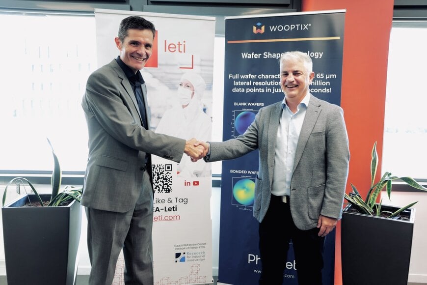
Wooptix installs automated inspection platform at CEA-Leti to advance nanotopography research.
wooptix.com
A new technical collaboration establishes the integration of automated wavefront phase imaging metrology within an industrial semiconductor cleanroom environment. The system utilizes automated spatial measurements to analyze wafer-scale process signatures, nanotopography, and advanced packaging parameters without compromising throughput constraints.
Technical challenges and collaboration rationale
Fabricating next-generation semiconductor devices requires highly precise process control to manage sub-nanometer topography variations across 300 mm wafers. As features shrink to nanoscale dimensions, traditional optical metrology tools face limitations in acquisition speed and spatial resolution, which are essential for detecting minute surface deformations.
To address these challenges, Wooptix and CEA-Leti combined their respective resources in wavefront phase imaging and advanced semiconductor research. The collaboration provides a vehicle to validate automated metrology platforms against complex process development challenges within a fully controlled, high-volume R&D facility.
System architecture and operational responsibilities
The deployment revolves around an automated metrology platform designed for high-volume semiconductor manufacturing environments. Wooptix provides the hardware architecture and measurement software, which delivers wafer shape and geometry data at sub-nanometer resolution.
Engineers at the CEA-Leti research institute manage the system integration within their cleanroom infrastructure. The technical team utilizes the platform to collect high-resolution data on wafer-scale process signatures, focusing on advanced packaging metrology and nanotopographic anomalies. The data collection supports ongoing research initiatives within European Union engineering frameworks to establish baseline parameters for advanced packaging.
Implementation and industrial deployment
The automated inspection system was installed within the cleanroom facilities in Grenoble, France, on May 4, 2026. The technical cooperation was formally reviewed during the CEA-Leti Innovation Days from June 23 to 25, 2026, in Grenoble.
The initial implementation phases focus on validating the tool's 300 mm automation platform under continuous production conditions. By inserting the system directly parallel to existing manufacturing processes, engineers are characterizing the tool's capability to identify surface deviations across diverse material interfaces without introducing chemical or mechanical contamination to the wafers.
Expected operational impact
Integrating wavefront phase imaging into the R&D pipeline enables precise tracking of mechanical stress and topography variations during thin-film deposition and chemical mechanical planarization steps. The sub-nanometer measurement resolution provides deterministic data that allows process engineers to optimize tool parameters and mitigate overlay errors. This analytical capability enhances process stability, improves overall yield predictability, and accelerates the development cycles of high-performance, complex semiconductor architectures.
Edited by Sucithra Mani, Induportals editor – adapted by AI.
www.wooptix.com
