
electronics-journal.com
12
'26
Written on Modified on
Hafnium Oxide-Based Ferroelectric Memory for Edge Computing Architectures
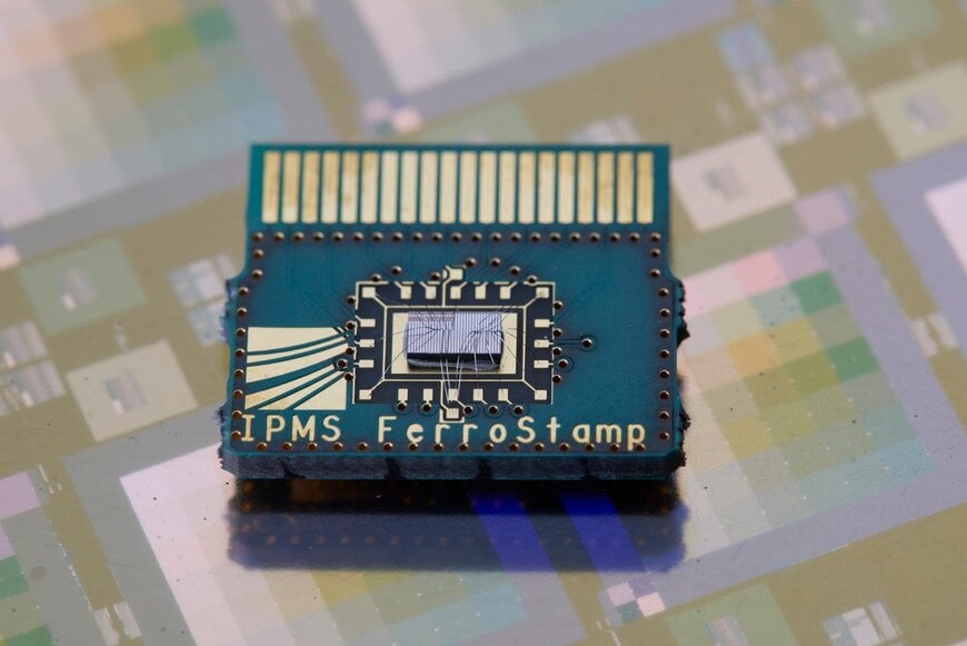
Fraunhofer IPMS and GlobalFoundries integrate non-volatile hafnium oxide memory into industrial semiconductor manufacturing processes.
www.fraunhofer.de
Energy savings, faster calculations and permanent data storage: The new storage technology meets all of these requirements.
Fraunhofer IPMS and GlobalFoundries have collaboratively developed a novel ferroelectric random-access memory (FRAM) technology based on hafnium oxide. The joint research project successfully integrated this ultra-fast, non-volatile memory into existing industrial semiconductor manufacturing nodes to support edge artificial intelligence, autonomous sensors, and low-power digital systems.
Ferroelectric Hafnium Oxide Architecture
The memory architecture utilizes ferroelectric hafnium oxide for permanent data storage. Within this ferroelectric memory technology, ions are shifted rapidly inside a crystal lattice to induce a change in polarization. This physical effect allows information to be stored and retained without an active power supply. The non-volatile cells can be read continuously without data loss, addressing the durability and high-speed requirements of the automotive, industrial automation, and medical technology sectors.
Industrial Manufacturing Integration
A primary engineering milestone of the project is the integration of these ferroelectric FRAM cells into GlobalFoundries' 22FDX technology node, a platform designed specifically for ultra-low-power microchips. The memory cells operate at sub-volt energy levels (less than one volt), execute switching operations within nanoseconds, and demonstrate a long cycle life capable of withstanding extensive write and erase cycles. This reproducible embedding process enables the large-scale industrial manufacturing of the memory arrays.
Power Consumption and Edge Computing
By significantly reducing power consumption compared to existing storage solutions, the hafnium oxide FRAM enables the deployment of artificial intelligence directly in edge applications where data is processed locally on the device. This low-power profile is critical for autonomous, battery-operated systems and on-board computing architectures that require high-performance data processing without relying on the latency or power overhead of centralized data centers.
Additional Context: This section details technical specifications and competitive benchmarking not included in the original product announcement
In the non-volatile memory sector, traditional ferroelectric RAM (FRAM) relies on complex perovskite materials such as lead zirconate titanate (PZT) or strontium bismuth tantalate (SBT). While offering high write speeds and endurance, these legacy materials are notoriously difficult to integrate into standard CMOS manufacturing facilities due to contamination risks (especially from lead) and severe scaling limitations below the 130nm node. The transition to hafnium oxide (HfO2)—a material already widely utilized in modern semiconductor fabs as a high-k dielectric for transistor gates—resolves these integration barriers. By crystallizing HfO2 into its ferroelectric phase, engineers can scale FRAM down to the 22nm node (such as the 22FDX process) and below, combining the high-speed, low-power characteristics of FRAM with the manufacturing scalability of standard silicon logic processes.
Edited by Lekshman Ramdas, Induportals editor – adapted by AI.
www.fraunhofer.de
