
electronics-journal.com
01
'26
Written on Modified on
3D Chip Stacking Advances AI Interconnect Density
CEA-Leti demonstrates ultra-fine die-to-wafer hybrid bonding technology designed to improve bandwidth and energy efficiency in advanced computing systems.
www.cea.fr
CEA-Leti has demonstrated a die-to-wafer (D2W) hybrid bonding process with interconnect pitches down to 1 μm, targeting performance limitations in artificial intelligence accelerators, high-performance computing systems, and advanced imaging devices. The results were presented at the Electronic Components and Technology Conference (ECTC) 2026 in Orlando, Florida, highlighting progress toward denser vertical integration in semiconductor packaging.
Die-to-Wafer Hybrid Bonding for Advanced Semiconductor Integration
As transistor scaling approaches physical and economic limits, semiconductor manufacturers are increasingly turning to advanced packaging and three-dimensional integration to continue improving computing performance. Rather than relying solely on smaller transistors, 3D integration enables multiple device layers to be vertically stacked, reducing the distance data must travel between components.
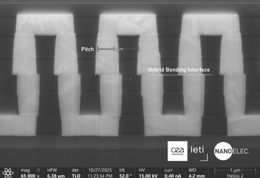
CEA-Leti's demonstration focused on die-to-wafer hybrid bonding, a technique that directly connects individual dies to a wafer using high-density copper-to-copper interconnections. By reducing interconnect pitch to 1 μm, the technology significantly increases the number of connections that can be placed within a given area.
For AI accelerators and high-performance computing systems, where memory bandwidth and data movement are major performance constraints, increasing interconnect density can improve communication between stacked devices while reducing energy consumption associated with data transfer.
Electrical Validation of Ultra-Fine-Pitch Interconnects
The research team reported successful electrical testing of structures containing up to 100,000 interconnect links. According to CEA-Leti, the results confirmed the viability of the hybrid bonding approach for high-density interconnect applications.
Electrical characterization of daisy-chain test structures demonstrated expected functionality and yield performance for pitches ranging from 5 μm down to 2 μm. The 1 μm structures also functioned successfully, although yields were constrained by the alignment accuracy of currently available bonding equipment.
The work represents an important step toward increasing vertical interconnect density in semiconductor systems where conventional package-level interconnect technologies may become limiting factors.
Alignment Accuracy and Wafer Reconstruction Challenges
Achieving a 1 μm pitch required addressing two key manufacturing challenges: alignment precision and surface planarization.
The primary technical hurdle involved positioning dies with sufficient accuracy during the bonding process. At sub-micron dimensions, even minor alignment deviations can affect electrical connectivity and yield.
The process also required wafer reconstruction through an inter-die gap filling (IDGF) technique. This step fills the spaces between adjacent dies before additional vertical interconnect structures are formed. To support subsequent process stages, the researchers optimized chemical mechanical planarization (CMP) to achieve the surface flatness required for reliable hybrid bonding and vertical interconnection.
These process refinements are intended to support future multi-die architectures with increasingly dense stacking configurations.
Integration with TSV and Through-Oxide Interconnect Technologies
The demonstrated D2W technology forms part of a broader semiconductor integration roadmap that includes high-density through-silicon vias (HD TSVs) and through-oxide vias (TOVs).
TSVs provide vertical electrical pathways through silicon substrates, while TOVs enable electrical routing through oxide layers. Combined with inter-die gap filling, these technologies can support wafer reconstruction and enable the integration of multiple dies performing different functions within a single stacked package.
Such architectures are becoming increasingly important in advanced AI systems, image sensors, and heterogeneous computing platforms where processors, memory, and specialized accelerators must exchange large amounts of data with minimal latency.
The ability to combine D2W and wafer-to-wafer (W2W) integration approaches may also provide greater flexibility in balancing performance, manufacturing yield, and production costs.
Roadmap Toward Sub-Micron Interconnect Scaling
CEA-Leti indicated that the current demonstration serves as a transitional proof-of-concept platform for future development.
The next phase of research will focus on integrating D2W bonding with HD TSV and TOV technologies while advancing toward a target pitch of 0.5 μm. According to the researchers, future bonding tools with alignment capabilities of approximately 0.5 μm (3σ) are expected to improve yield performance at these dimensions.
Reducing pitch further could enable substantially higher interconnect densities, supporting the growing bandwidth requirements of next-generation AI accelerators and advanced CMOS image sensors.
The research was conducted within the framework of the FAMES Pilot Line and the ANR NextGen project under the France 2030 initiative. Related work on inter-die gap filling, through-oxide vias, and high-density through-silicon vias received support from IRT Nanoelec.
Additional Context
This section details technical specifications and competitive benchmarking not included in the original news release.
The race to increase interconnect density has become a central focus of advanced semiconductor packaging. Comparable technologies include TSMC's SoIC (System on Integrated Chips), Intel's Foveros, Samsung's X-Cube, and hybrid bonding technologies developed by imec and other semiconductor research organizations.
Current advanced hybrid bonding technologies commonly operate in the low single-digit micron range, making a demonstrated 1 μm die-to-wafer hybrid bonding pitch a significant milestone in vertical interconnect scaling. As AI hardware architectures increasingly rely on chiplets and heterogeneous integration rather than traditional monolithic scaling, technologies enabling denser vertical interconnects are becoming critical components of the semiconductor supply chain. Improvements in interconnect density can increase bandwidth per unit area while reducing communication energy, two metrics that are increasingly important for AI accelerators, high-performance computing platforms, and advanced imaging systems.
Edited by Aishwarya Mambet, Induportals Editor, with AI assistance.
www.cea.com
