
electronics-journal.com
27
'26
Written on Modified on
Improved energy efficiency for high-demand applications
700V PowerGaN devices from STMicroelectronics improve energy efficiency and enable more compact power designs for AI servers, robotics, industrial systems and advanced consumer applications.
www.st.com
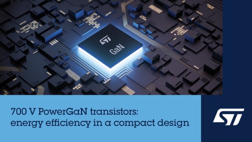
The implementation of wide-bandgap semiconductors serves as a foundational component in modern industrial power architectures and macro-scale electrification systems. Conventional silicon-based power conversion technologies face structural physical boundaries when subjected to the performance requirements of contemporary processing hardware and automated distribution networks. To address these thermal and electrical scaling constraints, integrated high-voltage semiconductor topologies are migrating toward gallium nitride configurations to handle intensive power distribution loads while increasing overall hardware power density.
Power Density and Thermal Regulation Parameters
Managing infrastructure power frameworks requires a combination of elevated switching frequencies and reduced electrical loss profiles. The integration of 700V PowerGaN transistors directly targets these high-power environments by minimizing internal conduction and switching degradation. Operating with an engineered 700V breakdown rating, these enhancement-mode devices maintain zero reverse-recovery charge, allowing power supply topologies to function smoothly at elevated switching cycles. By accelerating the permissible operational frequency, system hardware engineers can integrate smaller external passive elements and magnetic components, which concurrently optimizes space constraints and lowers overall operating temperatures.
This thermal and dimensional consolidation proves vital across a variety of dense infrastructural networks:
- Automated Robotics Systems: The compact footprint of the power conversion stage reduces individual component payload weight, extending structural articulation efficiency and localized thermal dissipation overhead in intensive mechanical environments.
- Smart-Grid Converters: High-voltage infrastructure nodes leverage low conduction losses to stabilize localized power generation, distribution, and energy storage routines while mitigating transmission degradation.
- Industrial Power Supplies: Consolidating high-voltage topologies into streamlined hardware stages enhances absolute reliability in continuous-use medium- and high-power applications.
Architectural Form Factors and Noise Immunity Mechanisms
The physical implementation of the 700V PowerGaN portfolio involves a matrix of surface-mount packaging structures designed to balance manufacturing cost and thermal outflux. The semiconductor line is divided across DPAK, TO-LL, and PowerFLAT 8x8 packaging architectures to permit direct drop-in integration into existing high-voltage board layouts. To suppress transient electrical noise during high-frequency cycles, the TO-LL and PowerFLAT options incorporate specialized Kelvin source connections.
This secondary internal connection separates the primary high-current power path from the delicate low-voltage gate-control loop. By decoupling these distinct electrical streams, the internal architecture maximizes absolute noise immunity, safeguards the driving circuitry, and preserves necessary timing margins during high-speed switching transitions. Consequently, infrastructure operators can implement these devices to directly handle rising artificial intelligence server power consumption and related data center power supply bottlenecks where operational continuity is vital.
Additional Context
This section details technical specifications and competitive benchmarking not included in the original news release.
High-voltage wide-bandgap power transistors are technically evaluated using a normalized Figure of Merit defined as the product of gate charge and on-resistance, alongside continuous current-carrying capacity under sustained thermal saturation. Legacy silicon superjunction MOSFETs, such as Infineon CoolMOS series devices operating in comparable 600V to 700V thresholds, typically manifest a high Figure of Merit that restricts their optimal switching frequencies below 100 kHz due to severe frequency-dependent parasitic losses and mandatory reverse-recovery delays.
The 700V PowerGaN series alters this operational benchmark by deploying seven distinct enhancement-mode high-electron-mobility transistor (HEMT) models covering a broad continuous current span from 6 A to 29 A.
Compared to competing standalone wide-bandgap solutions like Navitas Semiconductor’s GeneSiC or GaN Systems’ legacy discrete components, which frequently demand external negative gate-drive voltages to prevent accidental turn-on spikes, STMicroelectronics’ true enhancement-mode (normally-off) topology operates safely with standard gate driver configurations. This structural integration ensures the devices routinely exceed a 1 MHz switching frequency threshold while eliminating reverse-recovery losses entirely, defining a highly efficient baseline for high-density power supply infrastructures.
Edited by Romila DSilva, Induportals Editor, with AI assistance.
The physical implementation of the 700V PowerGaN portfolio involves a matrix of surface-mount packaging structures designed to balance manufacturing cost and thermal outflux. The semiconductor line is divided across DPAK, TO-LL, and PowerFLAT 8x8 packaging architectures to permit direct drop-in integration into existing high-voltage board layouts. To suppress transient electrical noise during high-frequency cycles, the TO-LL and PowerFLAT options incorporate specialized Kelvin source connections.
This secondary internal connection separates the primary high-current power path from the delicate low-voltage gate-control loop. By decoupling these distinct electrical streams, the internal architecture maximizes absolute noise immunity, safeguards the driving circuitry, and preserves necessary timing margins during high-speed switching transitions. Consequently, infrastructure operators can implement these devices to directly handle rising artificial intelligence server power consumption and related data center power supply bottlenecks where operational continuity is vital.
Additional Context
This section details technical specifications and competitive benchmarking not included in the original news release.
High-voltage wide-bandgap power transistors are technically evaluated using a normalized Figure of Merit defined as the product of gate charge and on-resistance, alongside continuous current-carrying capacity under sustained thermal saturation. Legacy silicon superjunction MOSFETs, such as Infineon CoolMOS series devices operating in comparable 600V to 700V thresholds, typically manifest a high Figure of Merit that restricts their optimal switching frequencies below 100 kHz due to severe frequency-dependent parasitic losses and mandatory reverse-recovery delays.
The 700V PowerGaN series alters this operational benchmark by deploying seven distinct enhancement-mode high-electron-mobility transistor (HEMT) models covering a broad continuous current span from 6 A to 29 A.
Compared to competing standalone wide-bandgap solutions like Navitas Semiconductor’s GeneSiC or GaN Systems’ legacy discrete components, which frequently demand external negative gate-drive voltages to prevent accidental turn-on spikes, STMicroelectronics’ true enhancement-mode (normally-off) topology operates safely with standard gate driver configurations. This structural integration ensures the devices routinely exceed a 1 MHz switching frequency threshold while eliminating reverse-recovery losses entirely, defining a highly efficient baseline for high-density power supply infrastructures.
Edited by Romila DSilva, Induportals Editor, with AI assistance.
