
electronics-journal.com
29
'26
Written on Modified on
Why SiC & GaN Power Semiconductors Are Becoming Harder to Test
Faster switching speeds and complex measurement conditions are increasing the need for accurate characterisation of wide-bandgap power devices.
induportals-media-publishing.com
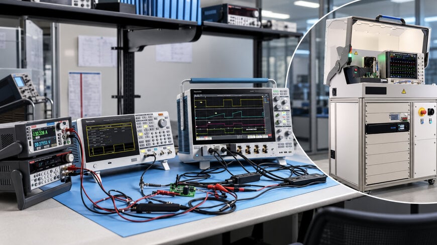
Wide-bandgap characterisation set-up: oscilloscopes, probes and signal sources on the test bench, with an automated double-pulse test system (inset).
Silicon carbide (SiC) and gallium nitride (GaN) power semiconductors are enabling more efficient and compact power conversion systems. They are increasingly used in electric vehicle inverters, fast chargers, industrial power electronics and data centre power supplies, and that growth is increasing the need for accurate switching characterisation.
Faster switching also brings new measurement challenges. Engineers must capture rapid voltage and current transitions without introducing distortion that could affect the evaluation of device performance. Specialised test and measurement systems are therefore becoming more important for characterising these devices under demanding electrical conditions.
Current Technology Market Landscape
Silicon has a bandgap of about 1.12 eV. Wide-bandgap semiconductors have bandgaps two to three times greater: around 3.3 eV for SiC and 3.4 eV for GaN. This gives them much higher breakdown electric fields, higher temperature limits and the ability to switch faster than conventional silicon devices.
SiC MOSFETs are particularly suited to high-voltage applications such as electric vehicle traction inverters and industrial power conversion. Automotive remains the largest driver of SiC demand. 800 V platforms are expected to make up about half of global battery electric vehicle shipments by 2031, and these platforms need much more SiC content than earlier 400 V designs.
GaN devices are widely used in high-frequency applications, including compact chargers and power supplies. Consumer and mobile electronics are expected to remain GaN's largest segment, reaching $1.7 billion in 2031. Automotive GaN, driven by onboard chargers and 48 V architectures, is forecast to grow at a 57% CAGR.
Silicon carbide (SiC) and gallium nitride (GaN) power semiconductors are enabling more efficient and compact power conversion systems. They are increasingly used in electric vehicle inverters, fast chargers, industrial power electronics and data centre power supplies, and that growth is increasing the need for accurate switching characterisation.
Faster switching also brings new measurement challenges. Engineers must capture rapid voltage and current transitions without introducing distortion that could affect the evaluation of device performance. Specialised test and measurement systems are therefore becoming more important for characterising these devices under demanding electrical conditions.
Current Technology Market Landscape
Silicon has a bandgap of about 1.12 eV. Wide-bandgap semiconductors have bandgaps two to three times greater: around 3.3 eV for SiC and 3.4 eV for GaN. This gives them much higher breakdown electric fields, higher temperature limits and the ability to switch faster than conventional silicon devices.
SiC MOSFETs are particularly suited to high-voltage applications such as electric vehicle traction inverters and industrial power conversion. Automotive remains the largest driver of SiC demand. 800 V platforms are expected to make up about half of global battery electric vehicle shipments by 2031, and these platforms need much more SiC content than earlier 400 V designs.
GaN devices are widely used in high-frequency applications, including compact chargers and power supplies. Consumer and mobile electronics are expected to remain GaN's largest segment, reaching $1.7 billion in 2031. Automotive GaN, driven by onboard chargers and 48 V architectures, is forecast to grow at a 57% CAGR.
Characterising these devices requires more than conventional electrical measurements. Engineers need to evaluate switching losses, voltage overshoot, current transients, reverse recovery and, for applicable devices, dynamic on-resistance. This demand is creating opportunities for high-bandwidth oscilloscopes, specialised voltage and current probes, integrated double-pulse test systems and automated characterisation software.
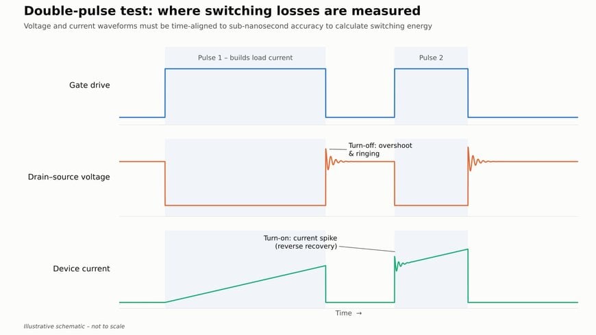
Double-pulse test waveforms: gate drive, drain–source voltage and device current, showing turn-off overshoot and turn-on reverse recovery (illustrative)
Core Market Challenge
The main challenge is to measure accurately without letting the test setup change the device behaviour being observed.
Wide-bandgap devices can switch in a few nanoseconds, and GaN transitions can exceed 100 V/ns. Edges this fast create voltage overshoot and ringing through even a few nanohenries of parasitic inductance in the circuit. Probe capacitance, insufficient bandwidth and timing mismatches between voltage and current channels can introduce further errors. As a rule of thumb, the measurement bandwidth required is about 0.35 divided by the rise time, so a 1 ns edge needs at least 350 MHz. In practice, engineers often choose instruments with three to five times that figure.
Double-pulse testing (DPT) is the industry-standard method for evaluating switching behaviour under controlled conditions. A first pulse builds up a defined current in an inductive load. After a short delay, a second pulse forces the device through a turn-off and turn-on transition at that current and voltage. Calculating switching energy from these events requires precise alignment of the voltage and current waveforms. Even a sub-nanosecond timing error can noticeably distort the result.
Wide-bandgap devices can switch in a few nanoseconds, and GaN transitions can exceed 100 V/ns. Edges this fast create voltage overshoot and ringing through even a few nanohenries of parasitic inductance in the circuit. Probe capacitance, insufficient bandwidth and timing mismatches between voltage and current channels can introduce further errors. As a rule of thumb, the measurement bandwidth required is about 0.35 divided by the rise time, so a 1 ns edge needs at least 350 MHz. In practice, engineers often choose instruments with three to five times that figure.
Double-pulse testing (DPT) is the industry-standard method for evaluating switching behaviour under controlled conditions. A first pulse builds up a defined current in an inductive load. After a short delay, a second pulse forces the device through a turn-off and turn-on transition at that current and voltage. Calculating switching energy from these events requires precise alignment of the voltage and current waveforms. Even a sub-nanosecond timing error can noticeably distort the result.
GaN devices add further requirements, including dynamic on-resistance characterisation, which evaluates how the device's on-state resistance changes after high-voltage switching. High-speed switching also increases the risk of spurious gate turn-on in half-bridge circuits, which can lead to destructive shoot-through.
These challenges make low-parasitic test fixtures, suitable probes and repeatable measurement configurations increasingly important.
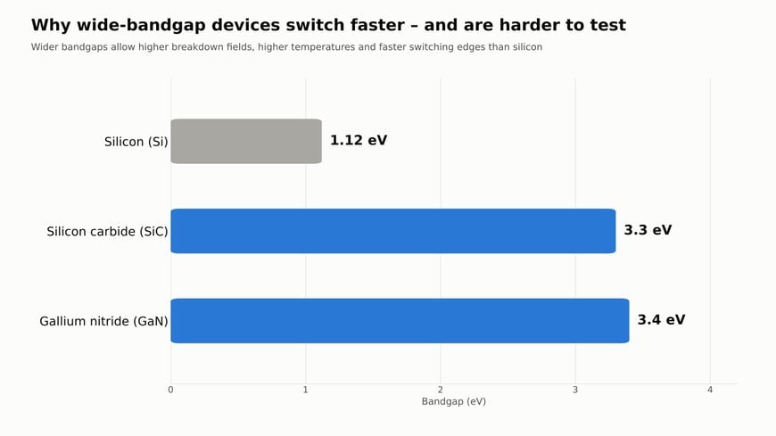
Bandgap comparison: silicon (1.12 eV), silicon carbide (3.3 eV) and gallium nitride (3.4 eV)
Existing Technology Solutions
Three leading test equipment manufacturers now offer integrated double-pulse platforms, but they differ widely in voltage, current and measurement range. Their published specifications give a useful picture of where each supplier is positioned.
Keysight Technologies' PD1500A Dynamic Power Device Analyzer / Double-Pulse Tester is a turnkey system for discrete SiC, GaN, silicon MOSFET and IGBT devices rated at 650 V, 1.2 kV and 1.7 kV. It tests at up to 1,200 V and 200 A, samples at 10 GSa/s and aligns voltage and current channels to within 200 ps. It accepts TO-247 and D2PAK-7 packages, tests at up to 175 °C (TO-247), and measures switching energy, reverse recovery, gate charge and on-resistance in line with IEC 60747-8/-9 and JESD24-10.
Tektronix's Wide Bandgap Double Pulse Test (WBG-DPT) Solution is built around the 8-channel MSO58B oscilloscope with 1 GHz bandwidth, running automated switching, timing and reverse-recovery measurements to JEDEC and IEC standards. The reference kit pairs it with a 400 MHz, ±2,000 V differential probe, a 120 MHz, 30 A current probe and an optional AFG31252 generator with built-in double-pulse software. Optional supplies cover 800 V or up to 2,000 V and 1,000 A, and the package includes three years of calibration and service.
Rohde & Schwarz's wide-bandgap characterisation solution, developed with PE-Systems, targets the high-power end of the market. The PE-Systems tester handles up to 2 kV (higher on request) and up to 3.6 kA, from 25 °C to 250 °C, or −55 °C to 250 °C with a ThermoStream add-on. The R&S RT-ZISO isolated probe reaches 1 GHz and ±3 kV with common-mode rejection above 90 dB at 1 GHz, which helps capture high-side signals cleanly.
These systems show equipment suppliers moving beyond individual instruments towards integrated characterisation platforms that cover the whole measurement process.
Actual Implementation on the Ground
Wide-bandgap semiconductor testing is relevant across several power electronics applications.
In electric vehicle traction inverters, SiC devices are evaluated for switching losses, voltage overshoot and thermal performance under high-voltage operating conditions. In compact chargers and high-frequency power supplies, GaN devices need accurate switching measurements and suitable test configurations.
AI data centres are now a significant new example. Rack power supplies are moving beyond 3 kW, and operators are shifting from 48/54 V rack distribution towards high-voltage DC architectures of up to 800 VDC (±400 V). Both SiC and GaN are being designed into these power stages. GaN revenue in telecom and infrastructure, driven largely by data centre demand, is forecast to grow at a 45% CAGR to $750 million in 2031. In these systems, small efficiency gains in each power stage add up across thousands of racks, so accurate switching-loss measurement directly affects design decisions.
Industrial motor drives, renewable energy converters and energy storage systems also rely on power semiconductor characterisation to assess efficiency, switching behaviour and electrical performance. However, test results depend on the device, test fixture, instruments and operating conditions. Gate-driver and transistor behaviour also shifts with temperature and load, so devices must be validated across their full operating range. A setup that is accurate for one device or application may not be for another.
Summary and Strategic Future Outlook
As SiC and GaN adoption accelerates, accurate, repeatable and application-specific testing is becoming more important. For test and measurement manufacturers, the opportunity lies in specialised probes, integrated double-pulse test platforms and automated characterisation software that reduce measurement uncertainty.
As power electronics move towards higher voltages, higher efficiency and greater power density, from 800 V vehicles to 800 VDC data centres, accurate measurement of switching behaviour will remain essential to semiconductor development, validation and commercialisation.
Edited by Sucithra Mani, Induportals editor – adapted by AI.
www.electronics-journal.com
As power electronics move towards higher voltages, higher efficiency and greater power density, from 800 V vehicles to 800 VDC data centres, accurate measurement of switching behaviour will remain essential to semiconductor development, validation and commercialisation.
Edited by Sucithra Mani, Induportals editor – adapted by AI.
www.electronics-journal.com
